If you’re a KiCad user, as many of us here at Hackaday are, you’ll be elated to hear that KiCad 4.0 has just been released! If you’re not yet a KiCad user, or if you’ve given it a shot in the past, now’s probably a good time to give it a try. (Or maybe wait until the inevitable 4.0.1 bugfix version comes out.)
If you’ve been using the old “stable” version of KiCad (from May 2013!), you’ve got a lot of catching-up to do.
The official part footprint libraries changed their format sometime in 2014, and are all now hosted on GitHub in separate “.pretty” folders for modularity and ease of updating. Unfortunately, this means that you’ll need to be a little careful with your projects until you’ve switched all the parts over. The blow is softened by a “component rescue helper” but you’re still going to need to be careful if you’re still using old schematics with the new version.
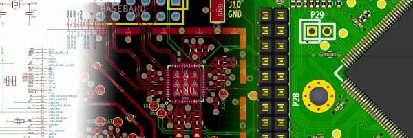
The most interesting change, from a basic PCB-layout perspective, is the push-and-shove router. We’re looking for a new demo video online, but this one from earlier this year will have to do for now. We’ve been using various “unstable” builds of KiCad for the last two years just because of this feature, so it’s awesome to see it out in an actual release. The push-and-shove router still has some quirks, and doesn’t have all the functionality of the original routers, though, so we often find ourselves switching back and forth. But when you need the push-and-shove feature, it’s awesome.
If you’re doing a board where timing is critical, KiCad 4.0 has a bunch of differential trace and trace-length tuning options that are something far beyond the last release. The 3D board rendering has also greatly improved.
Indeed, there are so many improvements that have been made over the last two and a half years, that everybody we know has been using the nightly development builds of KiCad instead of the old stable version. If you’ve been doing the same, version 4.0 may not have all that much new for you. But if you’re new to KiCad, now’s a great time to jump in.
We’ve covered KiCad hacks before, and have another article on KiCad add-on utilities in the pipeline as we write this. For beginners, [Chris Gammell]’s tutorial video series is still relevant, and is a must-watch.
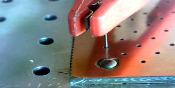
If you’ve ever made double-sided PCBs without professional equipment, you had to deal with connecting one side of the board to the other. You have a few obvious choices: 1) Rely on component leads to connect both sides (and solder both sides); 2) Create vias and solder wire to both sides of the board; or 3) Use through hole rivets. [Diyouware] had a different idea: use conductive ink. After a few false starts, they found a technique that seemed to work well.
This isn’t the first time we’ve heard of people trying conductive ink with varying degrees of success. The biggest problem, usually, is that the ink wants to run out of the hole. [Diyouware] has an interesting solution for this problem: Don’t drill the hole all the way thorough.
Everyone has their favorite process for PCB fabrication, as long as you’re a happy hacker I don’t think it really matters. But in this post I thought it might be interesting to describe my personal process, and some of the options available.
Making your own at home
The Dirty Electronics Skull Etching Synth a great looking maskless board.
Etching is the classic PCB fabrication option for the home hacker. It’s been many, many years since I etched a PCBs but it can produce interesting results. Some people don’t like it, and I’d personally tend to avoid it as a messy and finicky process. But, if you only need 1 or 2 layer boards with large features (through-hole components are best of course) it can be a viable option. In some cases, I think etched boards look awesome and are a great fit. One example is the skull etching shown to the right. The oxidation and discoloration of the boards adds to the design aesthetic in this case.
A simple design milled on an Accurate CNC
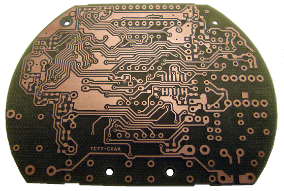
For those with a bigger budget a professional milling machine might be a viable choice. I’ve used an Accurate CNC in the past (LPKF and others make mills too), but this is an expensive option (no online pricing, but if $10,000 USD is a lot for you don’t bother). The accurate mill is pretty awesome, it can be fitted with a vacuum bed, automatic tool changer and vision system for alignment. The mill can produce high quality two layer boards with all the holes and vias drilled out. The final step of filling the vias is however manual, but compared to etched boards the results are pretty professional (the mill itself uses milled PCBs!). They claim a 0.1mm (4 mil) track size, I’ve never tried tracks this small but surface mount components were not a problem.
While a fun toy, it’s worth considering if you really need a PCB mill. The only case where they’re really valuable is if you want to be able to iterate over a design with less than a days turn around. This can be useful in RF or low noise designs where you might want to experiment with different layouts, but for other projects the price of a good mill can pay for quick turn around (1 or 2 days from order submission to delivery) on a lot of boards.
Commercial Fabrication
Years ago commercial fabrication used to be a very expensive and finicky process. For the most part you’d need to order a full panel putting the service outside of most hobbyists reach. Generating gerbers and drill files to the fabs specification could also be a process fraught with complication.
These days services that aggregate designs onto a single panel and break them out for distribution are common. For my work I mostly stick with OSHPark and SeeedStudio whose services complement each other well. I’ve also used Itead and found them compatible with Seeed (with the added benefit that they supply free boards for open projects).
Using OSHPark gives me the warm fuzzies. A child of the hacker community, born out of DorkbotPDX, all OSHPark’s boards are fabbed in the US (check out the great amphour interview for more details). Their services are limited to either 2 or 4 layer boards (always in purple, and always coated with gold (ENIG)), in 6×6 (6 mil traces with 6 mil spacing) or 5×5. I rarely attempt BGA boards so the 2 layer service works out great for me. OSHPark’s minimum order is 3 boards, which is perfect for prototyping. The gold plating also provides a nice finish, which both protects the board from oxidation and provides a nice surface to solder to. The main reason I use OSHPark however is that they’re cheap for small boards and have a relatively fast turn around (I recently purchased 3 tiny 20x15mm boards for $2.40 including shipping which was unbeatable). From OSHPark in the US to the UK my boards take about 2 weeks to arrive. They’ve also automatically upgrade boards to their super-swift service for free when there’s spare capacity. Their service is pretty slick, and provides a rendering of the gerbers prior to ordering as a final check which comes in very handy.
Seeed on the other hand are much cheaper for larger size boards and volume orders. They also provide more color and finishing options. The cheapest option at Seeed is green PCBs with HASL finish (hot air solder leveling). From Seeed, my boards usually take about a month to arrive (there are a few delivery options, but in my experience this is about as fast as it gets and faster shipping services often make using Seeed less attractive).
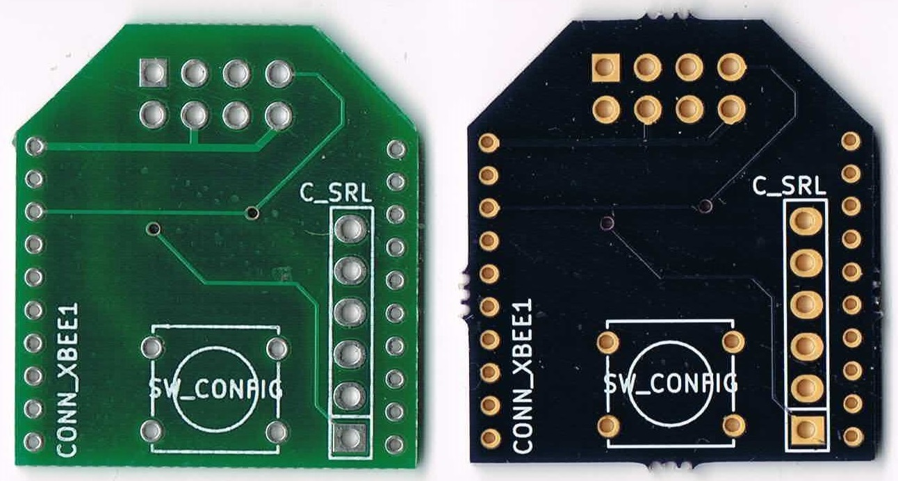
The image to the right shows a couple of very simple boards I had manufactured at both OSHPark and Seeed. I’ve never had a fabrication issues with boards from either service (though I prefer the ENIG finish).
Partly due to the limitations imposed by using commercial fabs I pipeline my projects. I send projects out to fab early in the design process and then switch to another design. When the board comes back I bring it up, bodge as required, and iterate over the layout. This works well with a two-week turn around, so I mostly use OSHPark while prototyping.
My boards also tend to be quite small (Arduino shield size or a little bigger). With small boards like this OSHPark is usually on-par or cheaper than ordering from Seeed (whose minimum quantity is 10 boards). With boards of about 100x100mm or larger I consider Seeed as they become significantly cheaper.
As a hobbyist I also rarely need huge numbers of boards, but for workshops when I need 10 or 20 boards I order from Seeed based on the final iteration of my prototypes. This is not only much cheaper than OSHPark, but I can get boards in a variety of colors to make workshops more interesting too.
This post has described some of the available options and my personal process. I hope it’s been interesting, but I’d love to hear about your favorite fabrication techniques, services and experiences both good and bad too. Please comment below!
Few things have had the impact on electronics that printed circuit boards (PCBs) have had. Cheap consumer electronics would not be as cheap if someone still had to wire everything (although by now we’d be seeing wiring robots, I’m sure). Between removing the human from the wiring process and providing many excellent electrical properties (at least, on a well-designed board), it isn’t surprising that even the cheapest examples of electronics now use PCBs.
For many years, the hallmark of being a big-time electronic hacker was the ability to make your own PCBs. There have been many ways that people have tried to bring PCB manufacturing into the hacker’s garage: stick on decals, light-sensitive blank PCBs, and even using laser printer toner (that last one spurred me to write a book on PCB layout many years back). You also see a lot of people using 3D printers or CNC mills to create PCBs. Hardly a week goes by that someone doesn’t ask me how to make a PCB in a home or small business lab.
Here’s an offer from Intel and the guy behind all of reality TV [Mark Burnett]: win a million dollars for making something. Pitch an idea for wearable electronics to the producers by October 2, and you might be on a reality TV show about building electronics which they’re calling America’s Greatest Makers. With this, Intel is promoting the Curie module a tiny, tiny SoC with Bluetooth, IMU, and DSP functions. We’re of the opinion that a Hackaday reader should win this contest, or at the very least be featured prominently in the show. No, it’s not Junkyard Wars, but it’s still a million dollar prize.
The Luka EV is a semifinalist for the Hackaday Prize, and a completely open, road legal electric vehicle powered by hub motors. It also looks really, really cool. Now, they’re selling them. It’s €20,000 for a complete car. Did I mention how cool it looks?
Boca Bearings is having a ‘Show Us Your Workshop’ contest, with the best (or should it be worst?) workshop winning tool cabinets, tool kits, a work mat, and calipers.
The EMU Drumulator is a classic drum machine that featured dirty 12-bit drum sounds in ROM. Now, it’s a single chip thanks to [Jan]. He’s done a lot of great work putting synths in single chips, and it’s great to see him move on to classic drum machines.
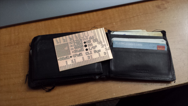
Hobby CNC mills have made rapid prototyping easier and faster for hackers. One really useful application is quickly fabricating your own milled PCB’s. [proto logical] built a Reference PCB Business Card using his CNC mill after repeatedly coming across other hackers who were not too convinced about the capabilities of CNC mills in routing PCB’s (also referred to as isolation milling). He thought of making a business card sized reference PCB to show around when he bumps into such folks.
To keep it useful, he included inch and centimetre scales, 0.1″ grid of holes, reference track widths from 16 mil to 66 mil, a few common drill holes and vias and some SMD foot prints. The single sided board is 50 mil thick, so it doesn’t bulk up his wallet. He’s posted the Eagle board file (direct download) and G-code (text file) for those interested in milling their own reference boards. The idea isn’t new – it’s been tried several times in different form factors in the past, generally using more traditional techniques. [proto logical] got inspiration from [Rohit Gupta’s] TinkerRule – The Maker’s Swiss Army Knife. Then there’s the very popular uRuler made by [Dave Jones] of EEVBlog fame. If you have any suggestions on improving the design, chime in with comments here.
Thanks to [ACG] for sending in this tip that he dug up while looking for CNC routed PCB’s.
We live in a golden age of free Electronic Design Automation (EDA) tools. It wasn’t that long ago that an engineering workstation was an expensive piece of hardware running very expensive software that typically had annual fees. Now, you can go to your local electronics store and buy a PC that would shame that old workstation and download plenty of software to design schematics, simulate circuits, program devices, and lay out PCBs.
The only problem with a lot of this free software is it runs on Windows. I do sometimes run Windows, but I most often use Linux, so there is a certain attractiveness to a new breed of tools that run in the Web browser. In particular, I wanted to look briefly at two Web-based EDA tools: EasyEDA and MeowCAD. Both offer similar features: draw a schematic, populate a PCB, and download manufacturing files (that is, Gerber files). EasyEDA also offers SPICE simulation.