copper-islands

Cutting Islands Into Copper-clad PCBs With A Drill

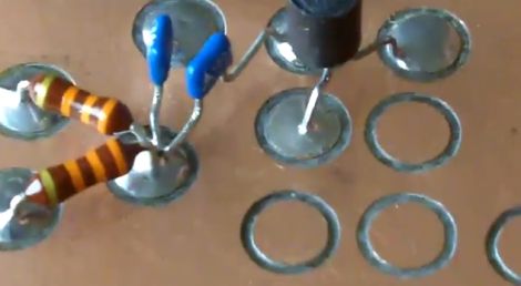
If you’re looking to build some small radio circuits, or if you are simply seeking a new look for your PCBs, you might want to check out what YouTube user [AndyDaviesByTheSea] has been working on lately. He has been building RF circuits as of late and was searching for a better way to create islands or “lands” on copper-clad PCBs.

He says that these sorts of islands are traditionally cut into the PCB with a scalpel or file – hardly an efficient process. [Andy] did a little experimenting and found a great way to quickly and precisely cut lands with a drill. Borrowing a bit of metal from an old VHS tape, he crafted a circular land cutter with a metal file. When mounted as a drill bit, his cutter produces clean, shallow cuts which create perfect lands on which to solder his components.

The only drawback to this method is that [Andy] found his bits were being dulled by the fiberglass boards pretty quickly. His solution was to carefully grind a broken heavy duty drill bit to do the task, which he says works even better than his original cutter.

Comparing Altium And Cadence PCB Layout Tools

We see a lot of projects using Eagle for the schematics and PCB layout. There are a few that use Kicad, but we hear very little about other alternatives. Recently, [Limpkin] has been working with Altium and Cadence and wrote about how they compare when it comes to PCB layout. Neither are free packages so it’s good to know what you’re getting into before taking the plunge.

[Limpkin] begins his overview by mentioning that the schematic editors are comparable; the differences start to show themselves in the PCB layout tools. Here you can see that Altium always labels the pads so you know what net each of them belongs to. Cadence (whose PCB layout tool is called Allegro) will display the net if you hover over the pad with your mouse. Both have 3D rendering, with Altium’s looking a bit more pleasant but what real use is it anyway? Okay, we will admit we love a good photorealistic board rendering, but we digress. The most interesting differences show themselves once traces are all on the board and need to be rejiggered. Cadence will actually move traces on other layers automatically to avoid collision with a via that is late to the party, and Altium shows some strange behavior when dragging traces. [Limpkin] doesn’t register a final judgement, but the comparison alone is worth the read.

The Many Iterations Of [Joe’s] PCB Business Card

[Joe Colosimo] is putting on a show with his PCB business card project. The idea isn’t new, but his goal is to keep it simple and undercut the cost of all other PCB cards he’s seen. This is the third generation of the board design, and he’s just waiting on some solder mask solution before he tries running it through the reflow oven.

The first two prototypes used some through-hole parts. Notably, the battery was to be positioned in a circular cut-out and held in place by a metal strap and some bare wires. But he couldn’t quite get it to work right so this design will transition to a surface-mount strap for one side, and the large circular pad for the other. At each corner of the board there is a footprint for an LED. He tried milling holes in the board to edge-light the substrate. Now he just mounts the LED upside down to give the board a blue glow. The LEDs are driven by an ATtiny10 microcontroller which takes input from the touch sensor array at the bottom right.

He etched a QR code on the board which seems to work better than the milled QR experiments we saw back in April. The link at the top point’s to [Joe’s] main page on the card. Don’t forget to follow the links at the bottom which cover each part of the development more in-depth.

[Thanks Skitchin]

Glass PCB LED Clock

This clock looks fantastic because of the glass PCB used for the build. This banner image allows you to see all the traces and components, but when it is lifted off of the desk surface the LEDs which make up the 7-segment digits appear to be floating.

The concept isn’t new, but it’s a much larger format than we’ve seen before. When we first looked at [CNLohr’s] glass PCB fabrication he was using microscope slides. This uses a much larger pane of glass but it seems the fabrication still uses copper foil glued to the glass, then toner transfer etched like normal.

Here he’s testing out some 74LV164 chips as constant current drivers. One of the commenters on the Reddit thread is skeptical about using the chip in this way and so are we. But as the video after the break shows, it seems to work (at least for now). [CNLohr] also mentions that the AVR soldered on the display is burnt out which doesn’t help his case. Still, we love the look and can’t wait to see where he goes from here!

Continue reading “Glass PCB LED Clock”

A Guide For Laying Out 4+ Layer PCBs

Learning to lay out a printed circuit board takes some time. But after you’ve churned out a few it’s really pretty easy. If you find yourself at that point it may be time to learn about more complicated board fabrication. We think a good primer is this multi-layer PCB layout guide which [Rik te Winkel] recently put together. It’s one of the results of his internship experience.

One of the major differences with boards that have more than two layers is the ability to alter what layers are actually connected by vias. Vias are plated holes through the substrate that connect different layers of copper. In the case of a 2-layer board these just go right through and connect the top to the bottom. But as you can see above, there are additional choices when it comes to multi-layer boards. #1 is a through via connecting all of the layers. #2 is a blind via; it stops part way through the board. And #3 is a buried via; it connects internal layers but cannot be seen from either side.

The guide is aimed at Eagle CAD. To use more than two layers you’ll have to purchase a license. But we think the concepts can easily be translated to other PCB layout software like Kicad.

An Interview With Laen (the Force Behind Dorkbot PDX)

[PT] recently interviewed [Laen], the man who makes it cheap and easy for hobbiests to have small PCBs manufactured. He created Dorkbot PDX’s PCB group order, a rapid turn PCB service which we see used in projects all the time (pretty much any purple PCB has gone through [Laen]).

Turns out his real name is [James Neal]. He’s a sysadmin by trade but deals in recreational circuitry at night. We were surprised to learn that the service has been rebranded. Its new name is OSH Park and it’s got a purple website with a new submission system. In the interview he discusses the genesis of the service. Inspired by a group parts order (that’s a mouthful!) with other hackers in Portland he saw a need for boards on which to mount them. The service has grown so much that he was spending 2-4 hours per night panelizing the designs. He made the wise choice to include an automated submission service in the new website that takes care of most of this work for him.

The rest of the interview spans a large range of topics. [Laen] shares his feelings on getting the boards manufactured domestically. He speaks briefly on the future of the service, and riffs on why open source hardware has value to him.

Repairing A Thermal Imaging Camera

[Mike] got his hands on this thermal imaging camera which is designed for use by Firefighters. As he’s demonstrating in the image above, it clips to a helmet and has a display what will let rescuers see through heavy smoke. But this one isn’t working right so he cracked it open and repaired the damaged board.

The hour-long video (embedded after the break) is quite interesting. He starts with a disassembly of the unit, before diving head-first into trouble shooting. There is a PCB inside that fills the entire U-shaped enclosure. The thermal sensor’s habit of cutting out seems to be a symptom of this design. There is one weak point where the board is very narrow. Flexing or vibrating that section will reset the sensor, and [Mike] ends up replacing a couple of components before the thing is fixed. These include a resistor and a ferrite bead both of which are suspected of having cracks due to that board flexing. The rest of the video is spent with an EEVblog-style look that the components and the construction.

Continue reading “Repairing A Thermal Imaging Camera”