We’re going to go out on a limb and predict that future history books will note that the decision to invade a sovereign nation straight after a worldwide pandemic wasn’t exactly the best timing. Turns out the global electronics shortage the pandemic helped to catalyze isn’t just affecting those of us with peaceful intentions, as the Russian war machine is having a few supply issues with the parts needed to build modern weapons and their associated control equipment.
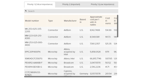
As you might expect, many of these parts are electronic in nature, and in some cases they come from the same suppliers folks like us use daily. This article from POLITICO includes an embedded spreadsheet, broken down by urgency, complete with part numbers, manufacturers, and even the price Moscow expects to pay!
Chips from US-based firms such as Texas Instruments are particularly hard for the Kremlin to source.
So what parts are we talking about anyway? The cheapest chip on the top priority list is the Marvell ‘Alaska’ 88E1322 which is a dual Gigabit Ethernet PHY costing a mere $7.10 USD according to Moscow. The most expensive is the 10M04DCF256I7G, which is an Altera (now Intel) Max-10 series FPGA, at $1,101 USD (or 66,815 Rubles, for those keeping score).
But it’s not just chips that are troubling them, mil-spec D-sub connectors by Airborn are unobtainable, as are all classes of basic passive parts, resistors, diodes, discrete transistors. Capacitors are especially problematic (aren’t they always). A whole slew of Analog Devices chips, as well as many from Maxim, Micrel and others. Even tiny logic chips from Nexperia.
Of course, part of this is by design. Tightened sanctions prevent Russia from purchasing many of these parts directly, which is intended to make continued aggression as economically unpleasant as possible. But as the POLITICO article points out, it’s difficult to prevent some intermediaries from ‘helping out’ without the West knowing. After all, once a part hits the general market, it is next to impossible to guarantee where it will eventually get soldered down.
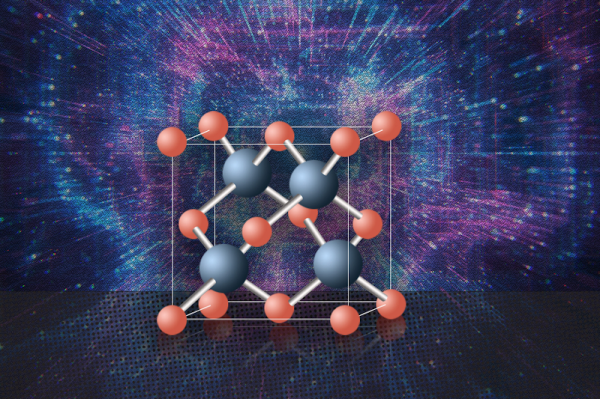
Silicon has had a long run as the king of semiconductors, and why not? It’s plentiful and works well. However, working well and working ideally are two different things. In particular, electrons flow better than holes through the material. Silicon also is a poor heat conductor as we’ve all noticed when working with high-speed or high-power electronics. Researchers at MIT, the University of Houston, and other institutions are proposing cubic boron arsenide to overcome these limitations.
According to researchers, this material is a superior semiconductor and, possibly, the best possible semiconductor. Unfortunately, the material isn’t nearly as common as silicon. Labs have created small amounts of the material and there is still a problem with fabricating uniform samples.
Early experiments show the material has very high mobility for electrons and holes along with thermal conductivity almost ten times greater than that of silicon. It also has a good bandgap, making it very attractive as a semiconductor material. In fact, only diamond and isotopically enriched cubic boron nitride have better thermal conductivity.
However, there are still unknowns about how to use the material in practical devices. Long-term stability tests are as lacking. So maybe it will wipe out silicon or maybe it won’t. Time will tell.
We’re used by now to many of the more capable microcontrollers and systems-on-chip that we use having an ARM core at their heart. From its relatively humble beginings in a 1980s British home computer, the RISC processor architecture from Cambridge has transformed itself into the go-to power-sipping yet powerful core for manufacturers far and wide. This has been the result of astute business decisions over decades, with ARM’s transformation into a fabless vendor of cores as IP at its heart. Recent news suggests that perhaps the astuteness has been in short supply of late though, as it’s reported that ARM’s Chinese subsidiary has gone rogue and detatched from the mothership taking the IP with it.
It seems that the CEO of the Chinese company managed to retain legal power when sacked by the parent company over questionable ties with another of his ventures, and has thus been able to declare it independent of its now-former parent. It still has the ARM IP up to the moment of detatchment and claims to be developing its own new products, but it seems likely that it won’t receive any new ARM IP.
What will be the effect of this at our level? Perhaps we have already seen it, as more Chinese chips such as the cheaper STM32 clones are likely to get low-end ARM cores as a result. It seems likely that newer ARM IP will remain for now in more expensive non-Chinese chip families, but in the middle of a semiconductor shortage it’s likely that we wouldn’t notice anyway. Where it will have a lasting effect is in future Chinese joint ventures by non-Chinese chip companies. Seeing ARM’s then-owner Softbank getting their fingers burned in such a way is likely to provide a disincentive to other companies considering a similar course. Whether ARM will manage to resolve the impasse remains to be seen, but it can hardly be a help to the rocky progress of their Nvidia merger.
After spending much of the 20th century languishing in development hell, electric cars have finally hit the roads in a big way. Automakers are working feverishly to improve range and recharge times to make vehicles more palatable to consumers.
With a strong base of sales and increased uncertainty about the future of fossil fuels, improvements are happening at a rapid pace. Oftentimes, change is gradual, but every so often, a brand new technology promises to bring a step change in performance. Silicon carbide (SiC) semiconductors are just such a technology, and have already begun to revolutionise the industry.
Mind The Bandgap
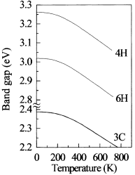
A graph showing the relationship between band gap and temperature for various phases of Silicon Carbide.
Traditionally, electric vehicles have relied on silicon power transistors in their construction. Having long been the most popular semiconductor material, new technological advances have opened it up to competition. Different semiconductor materials have varying properties that make them better suited for various applications, with silicon carbide being particularly attractive for high-power applications. It all comes down to the bandgap.
Electrons in a semiconductor can sit in one of two energy bands – the valence band, or the conducting band. To jump from the valence band to the conducting band, the electron needs to reach the energy level of the conducting band, jumping the band gap where no electrons can exist. In silicon, the bandgap is around 1-1.5 electron volts (eV), while in silicon carbide, the band gap of the material is on the order of 2.3-3.3 eV. This higher band gap makes the breakdown voltage of silicon carbide parts far higher, as a far stronger electric field is required to overcome the gap. Many contemporary electric cars operate with 400 V batteries, with Porsche equipping their Taycan with an 800 V system. The naturally high breakdown voltage of silicon carbide makes it highly suited to work in these applications.
If we had a dollar for every exciting new device that’s promised to change everything but we never hear of beyond the initial hoopla, we’d own our own private islands in the sun from the beaches of which we’d pick out Hackaday stories with diamond-encrusted keyboards. The electronic engineering press likes to talk about new developments, and research scientists like a bit of publicity to help them win their next grant.
The Bizen transistor however sounds as though it might have some promise. It’s a novel device which resembles a bipolar transistor in which the junctions exhibit Zener diode-like properties, and in which the mechanism is through quantum tunneling rather than more conventional means. If this wasn’t enough, its construction is significantly simpler than conventional semiconductors, requiring many fewer support components to make a logic gate than traditional CMOS or TTL, and requires only eight mask steps to manufacture. This means that lead times are slashed, and that the cost of producing devices is much reduced.
The device’s originator has partnered with a semiconductor fab house to offer a service in which custom logic chips can be produced using the new devices in a series of standard building blocks. This is likely to be only of academic interest to the hacker at the moment, however the prospect of this cost reducing as the technology matures does show promise of reaching the means of some more well-funded hacker projects. It will be a while before we can order a chip with the same ease as a PCB, but this makes that prospect seem just a little bit closer.
The semiconductor devices were put to the test under different atmospheres in this chamber.
One of the humbling things about writing for Hackaday comes when we encounter our readership and learn the breadth of our community and the huge variety of skills and professions you represent. Among your number are a significant representation among scientists, and as a result we often receive fascinating previews of and insights into their work. Sometimes they deserve a little bit more attention than one of our normal short daily pieces, and such a moment has come our way this week.
We’ve been fortunate enough to have an early look at a paper which makes detailed observations of a hitherto barely characterised property of semiconductor junctions that might have some interest for Hackaday readers in their work. In their paper, [Mellie], [Bacon] et al at Fulchester University in northeast England take a look at incandescent luminescence, a fleeting and curious effect exhibited by all semiconductor junctions in which they emit short-duration high-intensity infra-red and visible light with an extremely fast rise time when presented with high levels of current. This is a property which has been rarely exploited in commercial devices due to the large current densities required to reproduce it.
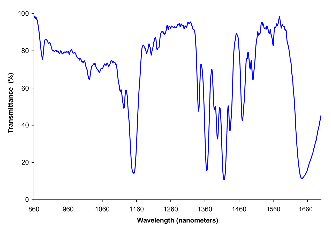
Incandescent Luminescence Explained
If you’ve never heard of incandescent luminescence before then you’re in good company, for neither had we until it was explained to us. It appears that there are a set of higher energy state conductivity bands in a semiconductor junction that can only be reached once the current passing through it breaches a threshold governed by the available quantum plasma dipole moment of the semiconductor material in question. At this point the junction assumes a plasma condition resulting in the abrupt emission of infra-red and visible radiation, the incandescent luminescence phase has been triggered.
A near-infra-red spectrum of incandescent luminescence in a silicon semiconductor junction.
Though it has been known to science since first being observed in the early 20th century by the earliest experimenters in the field of semiconductor junctions, the transitory nature of the phenomenon has traditionally been a barrier to its proper examination. The British team took a selection of commercial semiconductor devices very similar to the types that might be used by Hackaday readers, placed them in a chamber, and used an array of photoelectric sensors coupled with ionising detectors using americium-241 alpha radiation sources to measure their emissions.
The resulting data was then harvested for processing through a stack of custom high-speed ADC cards. Current densities from as low as a few milliamps to hundreds of amps were tested across forward-biased PN diode junctions using a computer-controlled DC power supply, resulting in a variety of spectra and showing the resulting thermionic photon emission at higher currents to have a preponderance in the infra-red region.
Incandescent luminescence in action, through an infra-red pyrometer.
A series of experiments were conducted to investigate a related effect first described by those early scientists in the field: that the atmosphere in which the semiconductor junction sits has a significant effect on the way it exhibits incandescent luminescence. Bathing it in gaseous CO₂ or nitrogen was found to reduce the phenomenon by as much as 95%, while immersing it in liquid nitrogen resulted in it becoming completely unobservable. Oxygen-rich atmospheres by comparison served to enhance the luminescence observed, to the point that in one of pure oxygen it reached an efficiency level of 100%.
The high conversion efficiencies and rapid onset of incandescent luminescence once it has been triggered compares favourably to those of existing devices such as LEDs or wire-wound resistors used where either infra-red or visible light is required. The researchers expect the effect to be exploited in such product families as photographic flash generators, electronic igniters, and other short-duration high-intensity applications. Given their obvious advantages, we’d expect their effects on those particular markets to be nothing short of incendiary.
Thanks Ellie D. Martin-Eberhardt for some invaluable inspiration and technical help with covering this story.
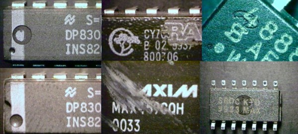
If you order an electronic component, how do you know what it is you are receiving? It has the right package and markings, but have you got the real thing from the original manufacturer or have you got an inferior counterfeit? We hear so much about counterfeit parts, and sometimes the level of effort put in by the fraudsters is so high that from either a visual or electrical standpoint they can be hard to spot.
The first feature of a package to be examined are the indents. Relabeled chips often have their old markings sanded off and a coating applied to simulate the surface of an unmolested chip, and this coating can either obliterate or partially fill any indentations. Using comparison photos we are shown discernable hidden indents, and partially filled indents.
We’re shown textures and paints, and how markings can sometimes be shown as counterfeit by washing with solvent. A Cypress-marked part is found to be a cheaper Altera one under the paint, and other parts are shown with misaligned markings and markings placed over indents. Wildly varying countries of origin are claimed while seemingly retaining the same batch codes, an impossibility confirmed by manufacturers.
If you order your parts from legitimate distributors then it’s likely that what you receive will be the genuine article. However with the popularity of online auction sites and online bazaars the possibility has become ever more likely of being left with a counterfeit. Knowing some of these tips might just make the difference between the success or failure of your work, so it’s an interesting read.