Admit it, you love looking at silicon die shots, especially when you have help walking through the functionality of all the different sections. This one’s really easy for a couple of reasons. [electronupdate] pointed his microscope at the die on a WS2812.
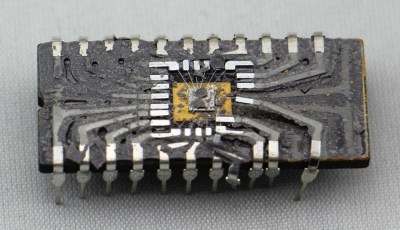
The WS2812 is an addressible RGB LED that is often called a Neopixel (a brand name assigned to it by Adafruit). The part is packaged in a 5×5 mm housing with a clear window on the front. This lets you easily see the diodes as they are illuminated, but also makes it easy to get a look at the die for the logic circuit controlling the part.
This die is responsible for reading data as it is shifted in, shifting it out to the next LED in the chain, and setting each of the three diodes accordingly. The funcitonality is simple which makes it a lot easier to figure out what each part of the die contributes to the effort. The diode drivers are a dead giveaway because a bonding wire connected to part of their footprint. It’s quite interesting to hear that the fourth footprint was likely used in testing — sound off in the comments if you can speculate on what those tests included.
We had no trouble spotting logic circuitry. This exploration doesn’t drill down to the gate level like a lot of [Ken Shirriff’s] silicon reverse engineering but the process that [electronupdate] uses is equally fun. He grabs a tiny solar cell and scopes it while the diodes are running to pick up on the PWM pattern used to fade each LED. That’s a neat little trick to keep in your back pocket for use in confirming your theories about clock rate and implementation when reverse engineering someone else’s work.
Continue reading “Closer Look At Everyone’s Favorite Blinky”


 We have most recently seen [Ken] at work