Those of use hailing from the UK may be quite familiar with the Royal Air Force’s Tornado fighter jet, which was designed to fight in a theoretical nuclear war, and served the country for over 40 years. This flying deathtrap (words of an actual serving RAF fighter pilot this scribe met a few years ago) was an extremely complex machine, with state-of-the-art tech for its era, but did apparently have a bit of a habit for bursting into flames occasionally when in the air!
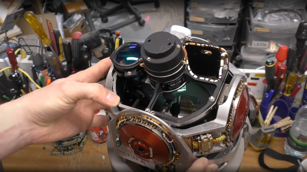
Anyway, the last fleet is now long retired and some of the tech inside it is starting to filter down into the public domain, as some parts can be bought on eBay of all places. [Mike] of mikeselectricstuff has been digging around inside the Tornado’s laser head unit, which was part of the bomber’s laser-guided missile subsystem, and boy what a journey of mechanics and electronics this is!

This unit is largely dumb, with all the clever stuff happening deep in an avionics bay, but there is still plenty of older high-end tech on display. Using a xenon-discharge-tube pumped yttrium aluminum garnet (YAG) laser, operating in pulsed mode, the job of the unit is to illuminate the ground target with an IR spot, which the subsequently fired missiles will home on to.
Designed for ground-tracking, whilst the aircraft is operating at speed, the laser head has three degrees of moment, which likely is synchronized with the aircraft movement to keep the beam steady. The optical package is quite interesting, with the xenon tube and YAG rod swimming in a liquid cooling bath, inside a metal housing. The beam is bounced around inside the housing using many prisms, and gated with a Q-switch which allows the beam to build up in intensity, before be unleashed on the target. Also of note is the biggest photodiode we’ve ever seen — easily over an inch in diameter, split into four quadrants, enabling the sensor to resolve direction changes in the reflected IR spot and track its error. A separate photodiode receiver forms part of the time-of-flight optical range finder, which is also important information to have when targeting.
There are plenty of unusual 3-phase positioning motors, position sensors, and rate gyros in the mix, with the whole thing beautifully crafted and wired-up military spec. It is definitely an eye opener for what really was possible during the cold war years, even if such tech never quite filtered down to civilian applications.
We’ve seen a few bits about the Tornado before, like this over-engineered attitude indicator, and here’s the insides of an old aircraft QAR (Quick Access Recorder)
Continue reading “Beautiful Engineering In This Laser Unit From A Tornado Jet Fighter”