Icestudio: An Open Source Graphical FPGA Tool

If you’ve ever worked with FPGAs, you’ve dealt with the massive IDEs provided by the vendors. Xilinx’s ISE takes about 6 gigabytes, and Altera’s Quartus clocks in at over 10 gigs. That’s a lot of downloading proprietary software just to make an LED blink.

[Jesús Arroyo]’s Icestudio is a new, graphical tool that lets you generate Verilog code from block diagrams and run it on the Lattice Semi iCEstick development board. A drag and drop interface lets you connect IOs, logic gates, dividers, and other elements. Once your block diagram is ready, a single button press downloads the code to the iCEstick.

Under the hood, Icestudio uses IceStorm, which we’ve discussed on HaD in the past, including this great talk by [Clifford], Icestorm’s lead. For the GUI, Icestudio uses nw.js, which spits out JSON based on the block diagram. This JSON is converted into a Verilog file and a PCF file. The Verilog is used to create the logic on the FPGA, and the PCF is used to define the pin configuration for the device. Clicking on selected modules reveals the generated Verilog if you want to know what’s actually going on.

It’s experimental, but this looks like a neat way to get started on FPGAs without learning a new language or downloading many gigs of toolchains. We’re hoping Icestudio continues to grow into a useful tool for education and FPGA development. A demo follows after the break.

[Thanks to Nils for the tip!]

Continue reading “Icestudio: An Open Source Graphical FPGA Tool”

Sort Faster With FPGAs

Sorting. It’s a classic problem that’s been studied for decades, and it’s a great first step towards “thinking algorithmically.” Over the years, a handful of sorting algorithms have emerged, each characterizable by it’s asymptotic order, a measure of how much longer an algorithm takes as the problem size gets bigger. While all sorting algorithms take longer to complete the more elements that must be sorted, some are slower than others.

For a sorter like bubble sort, the time grows quadradically longer for a linear increase in the number of inputs; it’s of order O(N²).With a faster sorter like merge-sort, which is O(N*log(N)), the time required grows far less quickly as the problem size gets bigger. Since sorting is a bit old-hat among many folks here, and since O(N*log(N)) seems to be the generally-accepted baseline for top speed with a single core, I thought I’d pop the question: can we go faster?

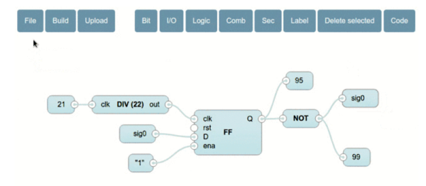
In short — yes, we can! In fact, I’ll claim that we can sort in linear time, i.e a running time of O(N). There’s a catch, though: to achieve linear time, we’ll need to build some custom hardware to help us out. In this post, I’ll unfold the problem of sorting in parallel, and then I”ll take us through a linear-time solution that we can synthesize at home on an FPGA.

Need to cut to the chase? Check out the full solution implemented in SystemVerilog on GitHub. I’ve wrapped it inside an SPI communication layer so that we can play with it using an everyday microcontroller.

To understand how it works, join us as we embark on an adventure in designing algorithms for hardware. If you’re used to thinking of programming in a stepwise fashion for a CPU, it’s time to get out your thinking cap!

Continue reading “Sort Faster With FPGAs”

FPGA To Ethernet Direct

When [iliasam] needed an Ethernet connection, he decided to see how much of the network interface he could put in the FPGA logic. Turns out that for 10 Base-T, he managed to get quite a bit inside the FPGA. His original post is in Russian, but automatic translation makes a passable attempt at converting to English.

This is a classic trade off all FPGA designers face: how much external logic do you use for a particular design. For example, do you add memory to the PCB, or use FPGA resources as memory? Each has its advantages and disadvantages (that’s why it is a trade off). However, if you are trying to keep things cheap, slashing external circuitry is often the way to go.

Continue reading “FPGA To Ethernet Direct”

PSoC VGA On A $10 Development Board

We’ve always found the Cypress PSoC an interesting beast. It’s a CPU with functional blocks that you can configure to build various I/O devices, including incorporating FPGA logic using Verilog. [MiguelVP] has an excellent multi-part project that produces VGA output from a PSoC. So far it just generates a fixed pattern, but a frame buffer is in the works, and there is plenty of detail about how to configure the PSoC for the task.

Although the PSoC has some analog capability, [MiguelVP] uses a cheap R2R DAC and VGA connector to interface to the VGA monitor. You can get the same PSoC board the project uses for about $10. The software, unfortunately, is Windows-only, so be prepared to fire up a virtual machine if you run Linux or Mac. Our own [Bil Herd] did a video introduction to PSoC that you can watch after the break.

Continue reading “PSoC VGA On A $10 Development Board”

Not Ready For FPGAs? Try A CPLD

[Kodera2t]  wanted to experiment with programmable logic. Instead of going with an FPGA board, he decided to build his own CPLD (complex programmable logic device) board, with a built-in programmer. The CPLD is a Xilinx 9536 which is inexpensive and, though obsolete, still readily available. The programmer for the board uses an FT232RL and the total cost is very low ([kodera2t] says it is in the price range of a Raspberry Pi Zero or about $4).

From a user’s point of view, a CPLD is just a small FPGA. Internally, there is a significant difference in how they implement your design. Although there are differences between different product families, CPLDs usually use a sea of logic gates arranged as an AND/OR chain. By feeding inputs and inverted inputs into the AND gates and then ORing the results, you can build interesting logic circuits. However, modern CPLDs use Verilog or VHDL, so you describe what you want just like with an FPGA and the software figures out how to use the underlying circuits to give you what you want.

Continue reading “Not Ready For FPGAs? Try A CPLD”

A Modern 386 Development Board

Some readers out there probably have nostalgic feelings for their first 386 based PC, the beeps and hisses of the modem, and the classic sound of a floppy drive’s stepper motor. Perhaps that turbo button that we could never quite figure out.

If you want the power of a 386 processor today, you’re in luck: [Pierre Surply] has developed a modern development board for the 80386SX CPU. This board is based on a 386 processor that comes in a LQFP package for “easy” soldering, and an Altera Cyclone IV FPGA.

To allow the CPU to run, the FPGA emulates the chipset you would usually find on a PC motherboard. The FPGA acts as both a bus controller and a memory controller for the CPU. On the board, there’s an SRAM chip and internal memory on the FPGA, which can be accessed through the 386’s bus access protocol.

The FPGA also provides debugging features. A supervisor application running on the FPGA gives debugging functionality via a FTDI USB to UART chip. This lets you control operation of the CPU from a PC for debugging purposes. The FPGA’s memory can be programmed through a JTAG interface.

The project is very well documented, and is a great read if you’re wondering how your old 386 actually worked. It can even be hand soldered, so the adventurous can grab the design files and give it a go. The francophones reading can also watch the talk in the video below.

Continue reading “A Modern 386 Development Board”