PSoC VGA On A $10 Development Board

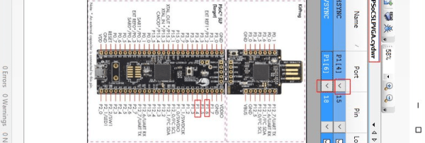
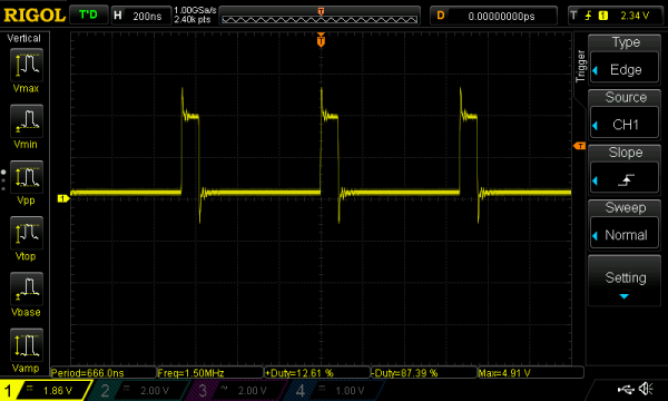
We’ve always found the Cypress PSoC an interesting beast. It’s a CPU with functional blocks that you can configure to build various I/O devices, including incorporating FPGA logic using Verilog. [MiguelVP] has an excellent multi-part project that produces VGA output from a PSoC. So far it just generates a fixed pattern, but a frame buffer is in the works, and there is plenty of detail about how to configure the PSoC for the task.

Although the PSoC has some analog capability, [MiguelVP] uses a cheap R2R DAC and VGA connector to interface to the VGA monitor. You can get the same PSoC board the project uses for about $10. The software, unfortunately, is Windows-only, so be prepared to fire up a virtual machine if you run Linux or Mac. Our own [Bil Herd] did a video introduction to PSoC that you can watch after the break.
Continue reading “PSoC VGA On A $10 Development Board” →

Not Ready For FPGAs? Try A CPLD

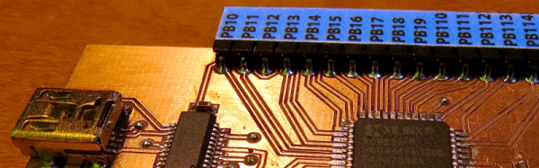
[Kodera2t]  wanted to experiment with programmable logic. Instead of going with an FPGA board, he decided to build his own CPLD (complex programmable logic device) board, with a built-in programmer. The CPLD is a Xilinx 9536 which is inexpensive and, though obsolete, still readily available. The programmer for the board uses an FT232RL and the total cost is very low ([kodera2t] says it is in the price range of a Raspberry Pi Zero or about $4).

From a user’s point of view, a CPLD is just a small FPGA. Internally, there is a significant difference in how they implement your design. Although there are differences between different product families, CPLDs usually use a sea of logic gates arranged as an AND/OR chain. By feeding inputs and inverted inputs into the AND gates and then ORing the results, you can build interesting logic circuits. However, modern CPLDs use Verilog or VHDL, so you describe what you want just like with an FPGA and the software figures out how to use the underlying circuits to give you what you want.

Continue reading “Not Ready For FPGAs? Try A CPLD” →

A Modern 386 Development Board

Some readers out there probably have nostalgic feelings for their first 386 based PC, the beeps and hisses of the modem, and the classic sound of a floppy drive’s stepper motor. Perhaps that turbo button that we could never quite figure out.

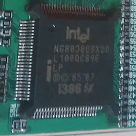
If you want the power of a 386 processor today, you’re in luck: [Pierre Surply] has developed a modern development board for the 80386SX CPU. This board is based on a 386 processor that comes in a LQFP package for “easy” soldering, and an Altera Cyclone IV FPGA.

To allow the CPU to run, the FPGA emulates the chipset you would usually find on a PC motherboard. The FPGA acts as both a bus controller and a memory controller for the CPU. On the board, there’s an SRAM chip and internal memory on the FPGA, which can be accessed through the 386’s bus access protocol.

The FPGA also provides debugging features. A supervisor application running on the FPGA gives debugging functionality via a FTDI USB to UART chip. This lets you control operation of the CPU from a PC for debugging purposes. The FPGA’s memory can be programmed through a JTAG interface.

The project is very well documented, and is a great read if you’re wondering how your old 386 actually worked. It can even be hand soldered, so the adventurous can grab the design files and give it a go. The francophones reading can also watch the talk in the video below.

Continue reading “A Modern 386 Development Board” →

Learn Flip Flops With (More) Simulation

In the previous installment, we talked about why flip flops are such an important part of digital design. We also looked at some latch circuits. This time, I want to look at some actual flip flops–that is circuit elements that hold their state based on some clock signal.

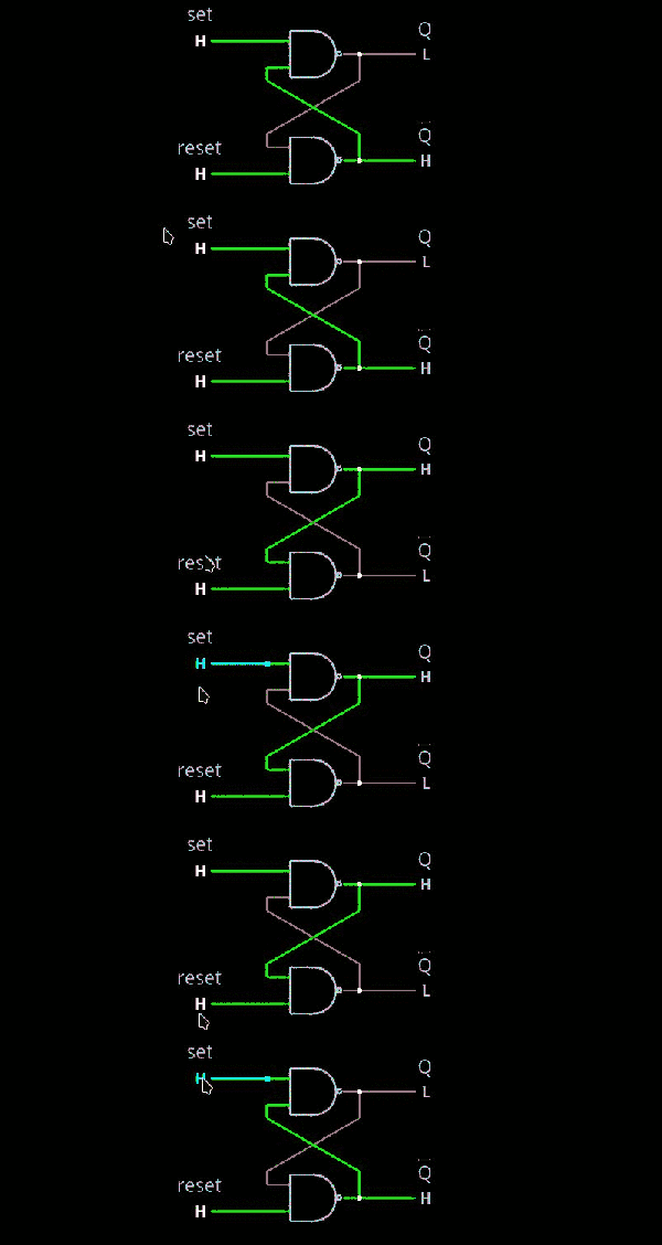
Just like last time, I want to look at sequential building blocks in three different ways: at the abstraction level, at the gate level, and then using Verilog and two online tools that you can also use to simulate the circuits. Remember the SR latch? It takes two inputs, one to set the Q output and the other to reset it. This unassuming building block is at the heart of many other logic circuits.

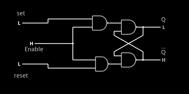
circ5A common enhancement to the SR latch is to include an enable signal. This precludes the output from changing when the enable signal is not asserted. The implementation is simple. You only need to put an additional gate on each input so that the output of the gate can’t assert unless the other input (the enable) is asserted. The schematic appears on the right.

In the case of this simulation (or the Verilog equivalent), the SR inputs become active high because of the inversion in the input NAND gates. If the enable input is low, nothing will change. If it is high, then asserted inputs on the S or R inputs will cause the latch to set or reset. Don’t set both high at the same time when the enable is high (or, go ahead–it is a simulation, so you can’t burn anything up).(Note: If you can’t see the entire circuit or you see nothing in the circuit simulator, try selecting Edit | Centre Circuit from the main menu.)

Continue reading “Learn Flip Flops With (More) Simulation” →

Learn Flip Flops With Simulation

Digital design with combinatorial gates like AND, OR, and NOT gates is relatively straightforward. In particular, when you use these gates to form combinatorial logic, the outputs only depend on the inputs. The previous state of the outputs isn’t important in combinatorial logic. While this is simple, it also prevents you from building things like state machines, counters, and even CPUs.

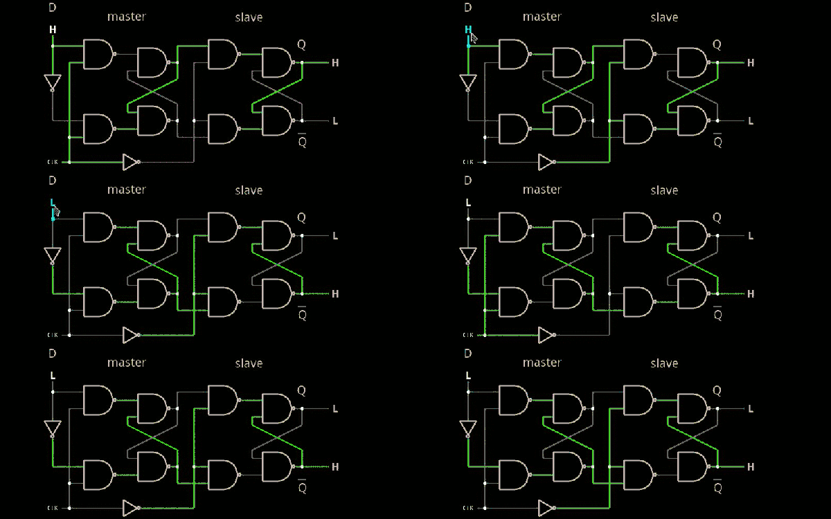
Circuits that use their own outputs as inputs are known as sequential circuits. It is true that at the fundamental level, sequential circuits use conventional logic gates. However, you usually won’t deal with them as gates, but will deal with abstractions like latches, flip flops, and even higher level constructs. Learning about these higher level constructs will allow you to make more advanced digital designs that are robust. In fact, if you are using an FPGA, building blocks like flip flops are essential since a large portion of the chip will be made up of some kind of flip flop.

Continue reading “Learn Flip Flops With Simulation” →

Learning Verilog For FPGAs: Hardware At Last!

Getting into FPGA design isn’t a monolithic experience. You have to figure out a toolchain, learn how to think in hardware during the design, and translate that into working Verliog. The end goal is getting your work onto an actual piece of hardware, and that’s what this post is all about.

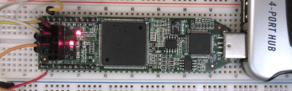
In the previous pair of installments in this series, you built a simple Verilog demonstration consisting of an adder and a few flip flop-based circuits. The simulations work, so now it is time to put the design into a real FPGA and see if it works in the real world. The FPGA board we’ll use is the Lattice iCEstick, an inexpensive ($22) board that fits into a USB socket.

Like most vendors, Lattice lets you download free tools that will work with the iCEstick. I had planned to use them. I didn’t. If you don’t want to hear me rant about the tools, feel free to skip down to the next heading.

Continue reading “Learning Verilog For FPGAs: Hardware At Last!” →