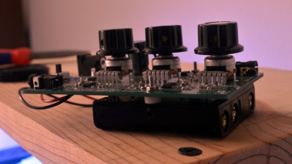
There was a time when any hi-fi worth its salt had a little row of sliders on its front panel, a graphic equalizer. On a hi-fi these arrays of variable gain notch filters were little more than a fancy version of a tone control, but in professional audio and PA systems they are used with many more bands to precisely equalise a venue and remove any unwanted resonances.
On modern hi-fi the task is performed in software, but [Grant Giesbrecht] wanted an analogue equalizer more in the scheme of those fancy tone controls than the professional devices. His project makes for a fascinating foray into analogue filter design, as well as an understanding of how an equalizer combines multiple filters. Unexpectedly their outputs are not mixed because it proves surprisingly difficult to ensure all the filters have the same gain, instead they are in series with the signal path passing through all filters.
The resulting equalizer is neatly built upon a PCB with a 4-AA-cell power supply, and makes for a self-contained audio component. Unexpectedly such analogue equalizer have been few and far between here at Hackaday so it’s particularly pleasing to see. We’re more used to graphical displays for off-the-shelf devices.
This summer’s Electromagnetic Field hacker camp in a field in western England gave many of the European side of our community their big fix of cool stuff for the year.
Some lucky individuals can spend the year as perpetual travelers, landing in a new country every week or so for the latest in the global round of camps. For the rest of us it is likely that there will be one main event each year that is the highlight, your annual fill of all that our global community has to offer. For many Europeans the main event was the biennial British event, Electromagnetic Field. From a modest start in 2012 this has rapidly become a major spectacle, one of the ones to include in your calendar, delivered both for our community and by our community.
If you search the web, you will learn that humans began to cook their food with fire a long time ago. Indeed, you might expect that there would be nothing new in the world of flame-based cookery. Fortunately [Bongodrummer] didn’t get that particular memo, because he’s created a rather unusual rocket stove griddle that is capable of cooking a significant quantity of food.
A rocket stove is designed to achieve as efficient use of energy as possible by achieving the most complete burn of high surface area fuel. It features a small combustion area and a chimney with supplementary air feed to ensure that exhaust gasses also burn. This one feeds all those hot gasses directly to the griddle, before taking them away up a pair of flues. As an added bonus there is a dome attachment for a pizza oven, made when a previous project had some left-over building material. Take a look at the comprehensive build video below the break.
Perhaps alarmingly the combustion chamber and chimney are made from a gas cylinder, but the use of a central heating radiator for the griddle is an extremely good idea. A vortex air inlet at the bottom and a secondary air injector further up the chimney complete the unit, making for a worthy replacement for a traditional barbecue.
In the over three decades since [Sophie Wilson] created the first ARM processor design for the Acorn Archimedes home computer, the architecture has been managed commercially such that it has become one of the most widely adopted on the planet. From tiny embedded microcontrollers in domestic appliances to super-powerful 64-bit multi-core behemoths in high-end mobile phones, it’s certain you’ll own quite a few ARM processors even if you don’t realise it. Yet none of those processors will have been made by ARM, instead the Cambridge-based company will have licenced the intellectual property of their cores to another semiconductor company who will manufacture the device around it to their specification. ARM core licences cost telephone-number sums, so unless you are a well-financed semiconductor company, until now you probably need not apply.
You will still have to shell out the dough to get your hands on a core for powerful chips like those smartphone behemoths, but if your tastes are more modest and run only to a Cortex M1 or M3 you might be in luck. For developers on Xilinx FPGAs they have extended the offer of those two processor cores at zero cost through their DesignStart Programme.
It’s free-as-in-beer rather than something that will please open-source enthusiasts, But it’s certainly a fascinating development for experimenters who want to take ARM for a spin on their own gate array. Speculation is swirling that this is a response to RISC-V, but we suspect it may be more of a partial lifting of the skirts to entice newbie developers such as students or postgraduates. If you arrive in the world of work already used to working with ARM IP at the FPGA level then you are more likely to be on their side of the fence when those telephone-number deals come up.
If you have a microcontroller to program, it can be an easy enough process to hook up a serial lead and perform the task. If however you have hundreds of microcontrollers on PCBs to program, connecting that lead multiple times becomes an impossibility. In manufacturing environments they have pogo pin jigs, an array of spring-loaded pins carrying the programming signals that line up perfectly with the appropriate pads on a PCB places on top of it.
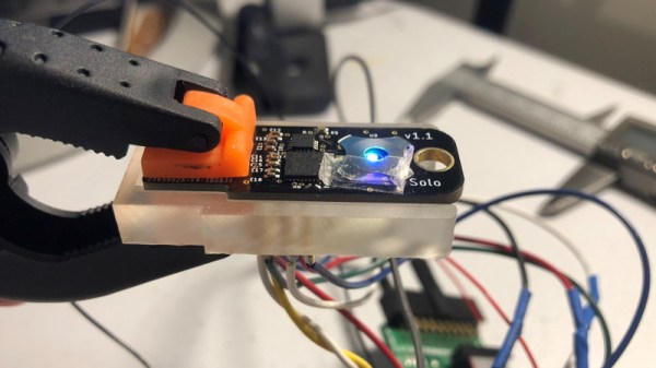
[Conor Patrick] is working on an upgrade to the U2F Zero 2-factor authentication token, and he faces exactly this problem of needing to program a lot of boards. His pogo pin jig is very nicely executed, and he’s taken us through his design and manufacture process for it.
Starting with his PCB design in Eagle, he exported it to Fusion 360 in which he was able to create a jig to fit it. Into the jig model he placed the holes for his chosen pogo pins in the appropriate places, before printing it with an SLA 3D printer. He is particularly complementary about the pins themselves, a solder bucket design that comes from mill-Max, and was sourced via DigiKey.
The proof of the pudding is in the eating, and happily when his completed jig received its first board, everything worked as planned and the programming proceeded flawlessly. We’ve shown you other pogo pin jigs, but this one is particularly nicely executed.
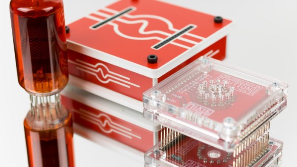
Nixie clocks, they’re a bit of a cliché, aren’t they? But still, they’re pretty to look at.
[Marcin Saj] has completely got our number, and with his Useless Nixie Device has stripped away any pretence of functionality from his Nixie and concentrated solely on the looking pretty part. It’s a box that steps through the display on any Nixie tube through the use of a set of pluggable socket modules, and it’s encased in an extremely attractive lase-cut acrylic enclosure. Internally it’s an extremely simple device, with a trusty 555 oscillator clocking a 4518 counter that in turn feeds 74141 driver. There is a MAX1771 boost converter in there too to create some high voltage for the tubes.
So it’s a pretty device and you can plug almost any Nixie into it given the right adapter. We guess it might be useful if you have a warehouse full of Nixies to test, but beyond that it’s a pretty desk toy. Still, it’s nice to see a Nixie project that’s not just another clock.
When you write a program for your computer, whether it is a desktop machine, a microcontroller, or a supercomputer, the chances are that you use software tools to help you get the job done. High level languages, compilers, linkers, assemblers, debuggers, and code libraries have become so integrated that in many cases you will barely be aware of their existence. To all intents and purposes this huge toolchain will be the computer. But the first computer programmers had none of these luxuries. They had to hand assemble their own binaries, check them by hand, and debug them by guessing what had happened when they failed.
EDSAC I, 1948, W.Renwick with 5 hole tape reader and Creed teleprinter. Copyright Computer Laboratory, University of Cambridge. Reproduced by permission. [CC BY 2.0 UK]EDSAC (Electronic delay storage automatic calculator) was the first computer operated by the University of Cambridge in the UK and one of the first few computers in the entire world when it was built in the late 1940s. It is the subject of the 1951 film you’ll find embedded below. Originally produced for a conference, the video sports a 1976 introduction and narration from the machine’s creator Professor Maurice Wilkes. It doesn’t take us through the design of the machine itself, instead it concentrates on the workflow required to program it.
The Paper-Heavy Process of Programming EDSAC
To illustrate the programming process, a committee of people who would now call themselves computer scientists, but probably then called themselves mathematicians, breaking a formula into subroutines before the code is laboriously hand assembled. The linking process is performed manually too by the secretary who types the code into a teletype for transfer to a punched tape. When a library function is required she reaches into a filing cabinet for the roll of tape containing it before running it through a tape duplicator to add it to the program. Finally the completed tape is checked and added to a job queue that consists of a row of hooks on the wall. Never complain that your toolchain is unwieldy again!
The original EDSAC was decommissioned in the late 1950s after serving the university and spawning a commercial version, the LEO, which became the first ever computer manufactured for use in commerce. That was not the end of the EDSAC story though, because in this century a team at the National Museum of Computing at Bletchley Park set about recreating EDSAC as an exhibit. And as luck would have it a member of that team was at the recent Electromagnetic Field hacker camp to give a talk about their work which you will also find below.
Building a Faithful Reproduction of EDSAC
Tony Abbey gives us both a history of the machine and a description of its architecture, followed by a run through their efforts in rebuilding it. You may be surprised by some of the unexpected facts from the talk. For instance, while all the tubes used in the EDSAC are still available, their bases are not. Equivalents were sourced from China, but team members had to modify them with dental drills.
They also needed to manufact the 1940s-style tube chassis, and the solution to that problem happened to be just down the road. Bletchley is part of modern-day Milton Keynes, a post-war new town that is also home to another famous name: Marshall amplifiers. Tube amps are built in a surprisingly similar way, so they took on the manufactured challenge. Not all the parts of the new EDSAC are original though. The memory used mercury delay lines in 1949, but for 2018 recreation the computer has a delay line using nickel wire and modern components. Tony admits that even that has caused problems, and there is a simulator using a microcontroller.


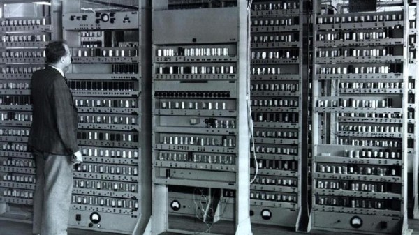
![EDSAC I, 1948, W.Renwick with 5 hole tape reader and Creed teleprinter. Copyright Computer Laboratory, University of Cambridge. Reproduced by permission. [CC BY 2.0 UK]](https://hackaday.com/wp-content/uploads/2018/09/edsac99-34.jpg)