Computer Vision For PCB Layout

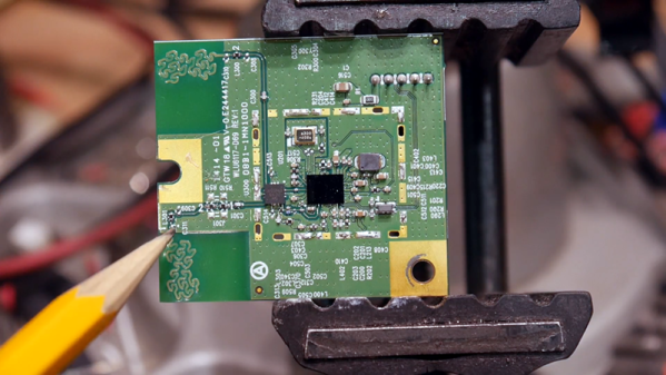
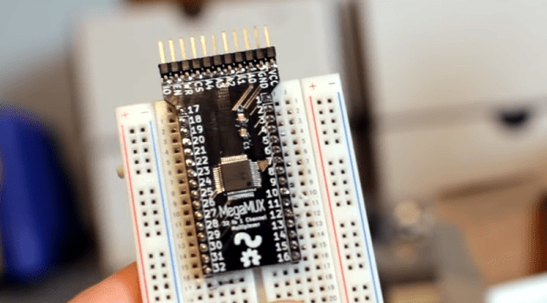
One of the big problems with doing PCB layout is finding a suitable footprint for the components you want to use. Most tools have some library although — of course — some are better than others. You can often get by with using some generic footprint, too. That’s not handy for schematic layout, though, because you’ll have to remember what pin goes where. But if you can’t find what you are looking for SnapEDA is an interesting source of components available for many different layout tools. What really caught our eye though was a relatively new service they have that uses computer vision and OCR to generate schematic symbols directly from a data sheet. You can see it work in the video below.

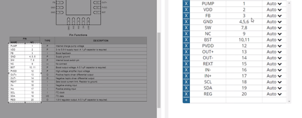
The service seems to be tied to parts the database already knows about. and has a known footprint available. As you’ll see in the video, it will dig up the datasheet and let you select the pin table inside. The system does OCR on that part of the datasheet, lets you modify the result, and add anything that it missed.

Continue reading “Computer Vision For PCB Layout”

Teardown Locates Fractal Antenna

[IMSAI Guy] tore apart a device with a wireless network card and decided to investigate what was under the metal can. You can see the video of his examination below. Overall, it was fairly unremarkable, but one thing that was interesting was its use of an antenna on the PCB that uses a fractal design.

You probably know fractals are “self-similar” in that they are patterns made of smaller identical patterns. The old joke is that the B. in Benoit B. Mandelbrot (the guy who coined the term fractal) stands for Benoit B. Mandelbrot. You can think of it as akin to recursion in software. Antennas made with fractal patterns have some unusual and useful properties.

Continue reading “Teardown Locates Fractal Antenna”

Getting Good At FPGAs: Real World Pipelining

Parallelism is your friend when working with FPGAs. In fact, it’s often the biggest benefit of choosing an FPGA. The dragons hiding in programmable logic usually involve timing — chaining together numerous logic gates certainly affects clock timing. Earlier, I looked at how to split up logic to take better advantage of parallelism inside an FPGA. Now I’m going to walk through a practical example by modeling some functions. Using Verilog with some fake delays we can show how it all works. You should follow along with a Verilog simulator, I’m using EDAPlayground which runs in your browser. The code for this entire article is been pre-loaded into the simulator.

If you’re used to C syntax, chances are good you’ll be able to read simple Verilog. If you already use Verilog mostly for synthesis, you may not be familiar with using it to model delays. That’s important here because the delay through gates is what motivates us to break up a lot of gates into a pipeline to start with. You use delays in test benches, but in that context they mostly just cause the simulator to pause a bit before introducing more stimulus. So it makes sense to start with a bit of background on delays.

Continue reading “Getting Good At FPGAs: Real World Pipelining”

Understanding A MOSFET Mixer

A mixer takes two signals and mixes them together. The resulting output is usually both frequencies, plus their sum and their difference. For example, if you feed a 5 MHz signal and a 20 MHz signal, you’d get outputs at 5 MHz, 15 MHz, 20 MHz, and 25 MHz. In a balanced mixer, the original frequencies cancel out, although not all mixers do that or, at least, don’t do it perfectly. [W1GV] has a video that explains the design of a mixer with a dual gate MOSFET, that you can see below.

The dual gate MOSFET is nearly ideal for this application with two separate gates that have effectively infinite input impedance. [Stan] takes you through the basic circuit and explains the operation in whiteboard fashion.

Continue reading “Understanding A MOSFET Mixer”

FPGA Persistently Rick Rolls You

When [Im-pro] wants a display, he wants it to spin.  So he built a persistence of vision (POV) display capable of showing a 12-bit color image of 131 x 131 pixels at 16 frames per second. You can see a video about the project below, but don’t worry, you can view it on your normal monitor.

The project starts with a Java-based screen capture on a PC. Data goes to the display wirelessly to an ESP8266. However, the actual display drive is done by an FPGA that drives the motor, reads a hall effect index sensor, and lights the LEDs.

Continue reading “FPGA Persistently Rick Rolls You”

High Voltage Switching With MOSFETs

Using a MOSFET as a switch is generally pretty simple. Make the gate voltage sufficient with respect to the source and current flows through the channel. However, if you are switching higher voltages, you may need some additional circuitry to protect the device’s gate and possibly the microcontroller driving the whole thing, too. [Lewis] discusses high voltage switching in the latest in his series of videos dealing with MOSFETs. You can see the video below.

You’ll see in the video a breadboard setup driving a 50 V load and also a higher-voltage H-bridge. There are three major topics covered: Using an optoisolator, using a gate bleeder resistor, and using a zener diode to limit gate voltage.

Continue reading “High Voltage Switching With MOSFETs”

Arduino Analog I/O Multiplexer

[SeanHodgins] has a project in mind where he needs to sample over 500 analog sensors. To get ready, he made a breakout board for 32-channel analog multiplexer device he wants to use. He put the project out on Hackaday.io and also has a video tutorial you can see below.

There are five input pins to the chip which lets you connect one analog pin to any one of 32 analog pins. Of course, in addition to the five control lines, you need some handshaking lines, too so you could use as many as eight digital pins to control the device.

Continue reading “Arduino Analog I/O Multiplexer”