Gates To FPGAs: TTL Electrical Properties

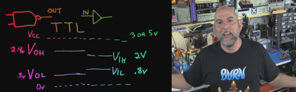
On the path to exploring complex logic, let’s discuss the electrical properties that digital logic signals are comprised of. While there are many types of digital signals, here we are talking about the more common voltage based single-ended signals and not the dual-conductor based differential signals.

Simulated "Real Life"
Single-ended Logic Signal

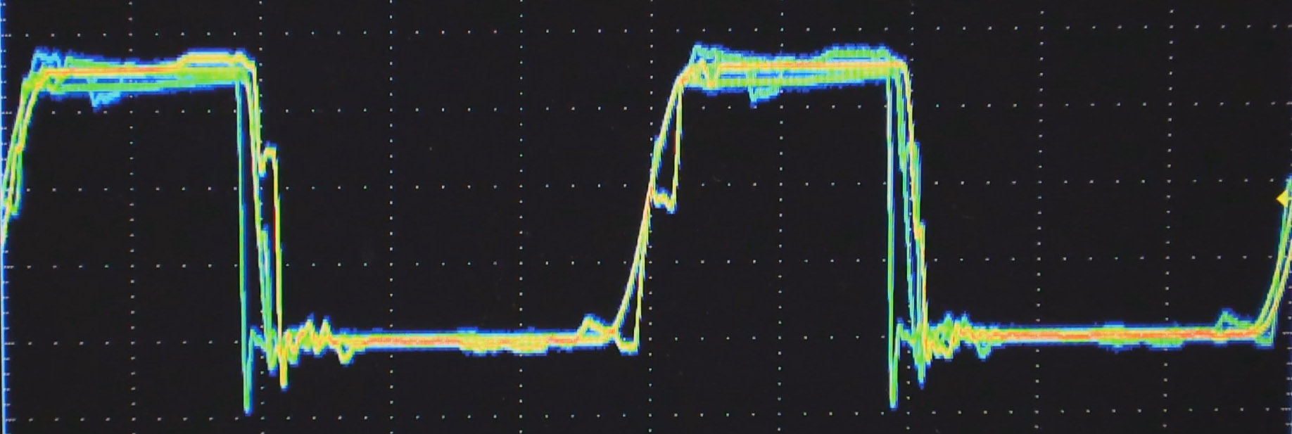
I think of most logic as being in one of two major divisions as far as the technology used for today’s logic: Bipolar and CMOS. Bipolar is characterized by use of (non-insulated gate) transistors and most often associated with Transistor Transistor Logic (TTL) based logic levels. As CMOS technology came of age and got faster and became able to drive higher currents it began to augment or offer an alternative to bipolar logic families. This is especially true as power supply voltages dropped and the need for low power increased. We will talk more about CMOS in the next installment.

TTL was a result of a natural progression from the earlier Resistor Transistor Logic (RTL) and Diode Transistor Logic (DTL) technologies and the standards used by early TTL became the standard for a multitude of logic families to follow.

Continue reading “Gates To FPGAs: TTL Electrical Properties”

From Gates To FPGA’s – Part 1: Basic Logic

It’s time to do a series on logic including things such as programmable logic, state machines, and the lesser known demons such as switching hazards. It is best to start at the beginning — but even experts will enjoy this refresher and might even learn a trick or two. I’ll start with logic symbols, alternate symbols, small Boolean truth tables and some oddball things that we can do with basic logic. The narrative version is found in the video, with a full reference laid out in the rest of this post.

Invert

1
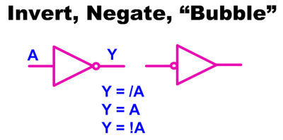
The most simple piece of logic is inversion; making a high change to low or a low change to high. Shown are a couple of ways to write an inversion including the ubiquitous “bubble” that we can apply almost anywhere to imply an inversion or a “True Low”. If it was a one it is now a zero, where it was a low it is now a high, and where it was true it is now untrue.

AND

2
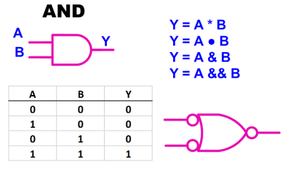
Moving on to the AND gate we see a simple truth table, also known as a Boolean Table, where it describes the function of “A AND B”. This is also our first opportunity to see the application of an alternate symbol. In this case a “low OR a low yields a low”

NAND

3
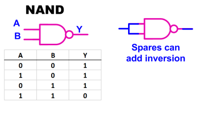
Most if not all of the standard logic blocks come in an inverted form also such as the NAND gate shown here. The ability to invert logic functions is so useful in real life that I probably used at least three times the number of NAND gates as regular AND gates when doing medium or larger system design. The useful inversion can occur as spares or in line with the logic.

Continue reading “From Gates To FPGA’s – Part 1: Basic Logic”

Interactive Software To Solve Crosstalk Problems

A link to this video demonstrating PCB cross-talk ended up in my mailbox the other day as I tend to stay on the mailing lists of the some of the high end CAD companies. There are some really interesting and powerful “mega-tools” that do things like plot noise density for decoupling analysis and extremely high speed timing analysis, though the costs of these tools are commensurate with their capabilities. This one is part of the Mentor Graphics PCB Simulation software.

The tool shown does the math needed to predict the induced voltage noise (cross-talk) generated by the proximity of noise sources to the noise susceptible elements, and the tool does so interactively. This is remarkable… in the past we would calculate some examples of trace width, spacing, and the type of signals involved, and then generate some rules of thumb that we tried to apply during the layout process. It was an educated guess that was sometimes not as close as we would have liked.

Virtual Scope Showing Predicted Crosstalk
Virtual Scope Showing Predicted Cross-talk


The cool part of this software is the interactive nature. One can learn the effects of placement on cross-talk in real time, which helps build an intuitive understanding.

I will add the standard disclaimer that a tool is exactly that, a tool, and it only represents an approximation of real life at best. It’s tempting to design to the tool itself, and many engineers have learned the limitation of a tool the hard way. Instead think of the tool as another opinion, or as mentioned, a learning aid to gather an intuitive feel for the effects of placement on circuit performance.

How To Build A Thermocouple Amplifier

A Thermocouple is a terrific way to measure temperature. The effects of temperature change on dissimilar metals produces a measurable voltage. But to make that measurement you need an amplifier circuit designed for the thermocouple being used.

Linear Technology LTC 1049 Low Power Zero-Drift Operational Amplifier with Internal Capacitors
Linear Technology LTC 1049 Low Power Zero-Drift Operational Amplifier
with Internal Capacitors

While researching “Zero Drift Amplifiers” as a follow-up to my video on Instrumentation Amplifiers I noticed the little schematic the front page of the LTC1049 datasheet which is shown here. I thought it was an ideal example of an analog application where some gain and some “gain helper” were needed to accomplish our useful little application of amplifying a thermocouple probe.

In the video I don’t really talk much about the thermocouples themselves other than the type I see most of the time which is type K. If you’re not already familiar with the construction of these probes you can find an informative write-up on thermocouples and the different types on the Wikipedia page and you might also want to check out the Analog Devices app note if you would like to know more. What I will cover is a reliable and precise way to read from these probes, seen in the video below and the remainder of the post after the break.

Continue reading “How To Build A Thermocouple Amplifier”

Instrumentation Amplifiers with Bil Herd

Instrumentation Amplifiers And How To Measure Miniscule Change

These days there a large number of sensors and analog circuits that are “controller friendly” meaning that their output signal is easily interfaced to the built-in Analog to Digital Convertors (ADCs) often found in today’s micro-controllers. This means that the signals typically are already amplified, often filtered, and corrected for offset and linearity. But when faced with very low level signals, or signals buried in a larger signal an Instrumentation Amplifier may be what’s needed. The qualities of an Instrumentation Amplifier include:

  • A differential amplifier with high impedance and low bias current on both inputs.
  • Low noise and low drift when amplifying very small signals.
  • The ability to reject a voltage that is present on both inputs, referred to as Common Mode Rejection Ratio (CMRR)

Continue reading “Instrumentation Amplifiers And How To Measure Miniscule Change”

Controlling Analog with SPI

We Assume Control: SPI And A Digital Potentiometer

In the last video I demonstrated a Universal Active Filter that I could adjust with a dual-gang potentiometer, here I replace the potentiometer with a processor controlled solid-state potentiometer. For those that are too young to remember, we used to say “solid-state” to differentiate between that and something that used vacuum tubes… mostly we meant you could drop it without it breakage.

The most common way to control the everyday peripheral chips available is through use of one of the common Serial Protocols such as I2C and SPI.  In the before-time back when we had only 8 bits and were lucky if 7 of them worked, we used to have to memory map a peripheral or Input/Output (I/O) controller which means we had to take many control and data lines from the microprocessor such as Data, Address, Read/Write, system clocks and several other signals just to write to a couple of control registers buried in a chip.

Nowadays there is a proliferation of microcontrollers that tend to have built-in serial interface capability it is pretty straightforward to control a full range of peripheral functions; digital and analog alike.  Rather than map each peripheral using said data and address lines,which is a very parallel approach,  the controller communicates with peripherals serially using but a handful of signal lines such as serial data and clock. A major task of old system design, mapping of I/O and peripherals, is no longer needed.

Continue reading “We Assume Control: SPI And A Digital Potentiometer”

Universal Active Filters part 2 for Hackaday by Bil Herd

Universal Active Filters: Part 2

An easy way to conceptualize active filters is thinking about audio speakers. A speaker crossover has a low-pass, high-pass and band-pass effect breaking a signal into three components based upon frequency. In the previous part of this series I took that idea and applied it to a Universal Active Filter built with a single chip opamp based chip known as the UAF-42. By the way, it’s pretty much an older expensive chip, just one I picked out for demonstration.

Using a dual-ganged potentiometer, I was able to adjust the point at which frequencies are allowed to pass or be rejected. We could display this behavior by sweeping the circuit with my sweep frequency function generator which rapidly changes the frequency from low to high while we watch what can get through the filter.

In this installment I’ll test the theory that filtering out the harmonics which make up a square wave results in a predictable degradation of the waveform until at last it is a sine wave. This sine wave occurs at the fundamental frequency of the original square wave. Here’s the video but stick with me after the break to walk through each concept covered.

Continue reading “Universal Active Filters: Part 2”