The one thing that separates the pros on Twitch from the dilettantes is the production values. It’s all about the smooth transitions, and you’ll never catch the big names fiddling with dodgy software mid-stream. The key to achieving this is by having a streamdeck to help control your setup, like this straightforward design from [Electronoobs]. (Video, embedded below.)
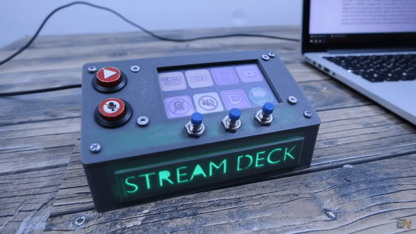
The build relies on an Arduino Micro, which is a microcontroller board perfectly equipped to acting as a USB macro keyboard. It’s paired with a Nextion LCD touchscreen that displays buttons for various stream control features, like displaying a “Be Right Back” screen or cuing up video clips. The build also features bigger regular buttons for important quick-access features like muting a mic. It’s all wrapped up in a 3D printed housing, with some addressable RGB LEDs running off another Arduino to add some pizazz. The neat trick is that the build sends keycodes for F13-F24, which allows for the streamdeck’s hotkeys to avoid conflicting with any other software using conventional keyboard hotkeys.
It’s a useful tool that would be of use to anyone streaming on Twitch or other platforms. Alternatively, you could repurpose an old phone to do a similar job. Video after the break.
Continue reading “DIY Streamdeck Helps You Professionalize Your Twitch Show”