There’s no doubting the wonders that micro-electromechanical systems (MEMS) technology have brought to the world. With MEMS chips, your phone can detect the slightest movement, turning it into a sensitive sensor platform that can almost anticipate what you’re going to do next. Actually, it’s kind of creepy when you think about it.
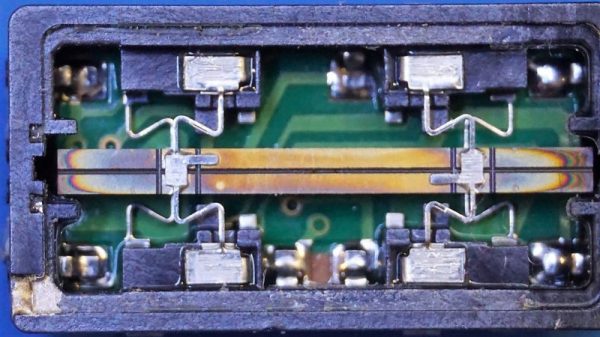
But before nano-scale MEMS inertial sensing came along, lots of products needed to know their ups from their downs, and many turned to products such as this vibrating piezoelectric gyroscope that [Kerry Wong] found in an old camcorder. The video below shows a teardown of the sensor, huge by MEMS standards but still a marvel of micro-engineering. The device is classified as a Coriolis vibratory gyroscope (CVG) which, as the name implies, uses the Coriolis effect to sense rotation. In this device, [Kerry] found that a long, narrow piezoelectric element spans the long axis of the sensor, suspended from what appears to be four flexible arms. [Kerry] probed the innards of the sensor while powered up and discovered a 22 kHz signal on the piezo element; this vibrates the bar in one plane so that when it rotates, it exerts a force on the support arms that can be detected. Indeed, [Kerry] hooked the output of the sensor to a wonderfully old-school VOM whose needle wiggled with the slightest movement of the sensor.
Sadly, MEMS made this kind of sensor obsolete, but we appreciate the look under the hood. And really, MEMS chips are using the same principle to detect motion, just on a much smaller scale. Want the MEMS basics? [Al] has you covered.
Continue reading “Piezoelectric Gyro Shows How They Rolled Back In The Day”