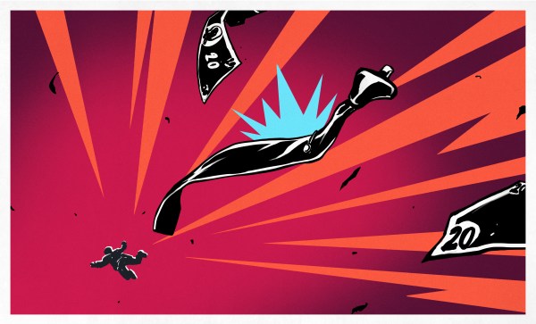
When Hacking And Biosensing Collide

[Prof. Edwin Hwu] of the Technical University of Denmark wrote in with a call for contributions to special edition of the open-access scientific journal Biosensors. Along the way, he linked in videos from three talks that he’s given on hacking consumer electronics gear for biosensing and nano-scale printing. Many of them focus on clever uses of the read-write head from a Blu-ray disc unit (but that’s not all!) and there are many good hacks here.

For instance, this video on using the optical pickup for the optics in an atomic force microscope (AFM) is bonkers. An AFM resolves features on the sub-micrometer level by putting a very sharp, very tiny probe on the end of a vibrating arm and scanning it over the surface in question. Deflections in the arm are measured by reflecting light off of it and measuring their variation, and that’s exactly what these optical pickups are designed to do. In addition to phenomenal resolution, [Dr. Hwu’s] AFM can be made on a shoestring budget!

Speaking of AFMs, check out his version that’s based on simple piezo discs in this video, but don’t neglect the rest of the hacks either. This one is a talk aimed at introducing scientists to consumer electronics hacking, so you’ll absolutely find yourself nodding your heads during the first few minutes. But then he documents turning a DVD player into a micro-strobe for high speed microfluidics microscopy using a wireless “spy camera” pen. And finally, [Dr. Hwu’s] lab has also done some really interesting work into nano-scale 3D printing, documented in this video, again using the humble Blu-ray drive, both for exposing the photopolymer and for spin-coating the disc with medium. Very clever!

If you’re doing any biosensing science hacking, be sure to let [Dr. Hwu] know. Or just tear into that Blu-ray drive that’s collecting dust in your closet.

Continue reading “When Hacking And Biosensing Collide”

Screenshot from the video in question, showing 12:54 of the video, demonstrating how the electrons are being exchanged when circuit is completed

Li-ion Battery Low-Level Intricacies Explained Excellently

There’s a lot of magic in Lithium-ion batteries that we typically take for granted and don’t dig deeper into. Why is the typical full charge voltage 4.2 V and not the more convenient 5 V, why is CC/CV charging needed, and what’s up with all the fires? [The Limiting Factor] released a video that explains the low-level workings of Lithium-ion batteries in a very accessible way – specifically going into ion and electron ion exchange happening between the anode and the cathode, during both the charge and the discharge cycle. The video’s great illustrative power comes from an impressively sized investment of animation, script-writing and narration work – [The Limiting Factor] describes the effort as “16 months of animation design”, and this is no typical “whiteboard sketch” explainer video.

This is 16 minutes of pay-full-attention learning material that will have you glued to your screen, and the only reason it doesn’t explain every single thing about Lithium-ion batteries is because it’s that extensive of a topic, it would require a video series when done in a professional format like this. Instead, this is an excellent intro to help you build a core of solid understanding when it comes to Li-ion battery internals, elaborating on everything that’s relevant to the level being explored – be it the SEI layer and the organic additives, or the nitty-gritty of the ion and electron exchange specifics. We can’t help but hope that more videos like this one are coming soon (or as soon as they realistically can), expanding our understanding of all the other levels of a Li-ion battery cell.

Last video from [The Limiting Factor] was an 1-hour banger breaking down all the decisions made in a Tesla Battery Day presentation in similarly impressive level of detail, and we appreciate them making a general-purpose insight video – lately, it’s become clear we need to go more in-depth on such topics. This year, we’ve covered a great comparison between supercapacitors and batteries and suitable applications for each one of those, as well as explained the automakers’ reluctance to make their own battery cells. In 2020, we did a breakdown of alternate battery chemistries that aim to replace Li-ion in some of its important applications, so if this topic catches your attention, check those articles out, too!

Continue reading “Li-ion Battery Low-Level Intricacies Explained Excellently”

Mining And Refining: From Red Dirt To Aluminum

No matter how many syllables you use to say it, aluminum is one of the most useful industrial metals we have. Lightweight, strong, easily alloyed, highly conductive, and easy to machine, cast, and extrude, aluminum has found its way into virtually every industrial process and commercial product imaginable.

Modern life would be impossible without aluminum, and yet the silver metal has been in widespread use only for about the last 100 years. There was a time not all that long ago that aluminum dinnerware was a status symbol, and it was once literally worth more than its weight in gold. The reason behind its one-time rarity lies in the effort needed to extract the abundant element from the rocks that carry it, as well as the energy to do so. The forces that locked aluminum away from human use until recently have been overcome, and the chemistry and engineering needed to do that are worth looking into in our next installment of “Mining and Refining.”

Continue reading “Mining And Refining: From Red Dirt To Aluminum”

A home-made colorimeter

Classic Colorimeter Clone Calibrates Cuvettes’ Contents

For anyone dabbling in home chemistry, having access to accurate measurement equipment can mean the difference between success and failure. But with many instruments expensive and hard to find, what’s a home chemist to do? Build their own equipment, naturally. [Abizar] went ahead and built himself a colorimeter out of wood and spare electronic components.

A colorimeter (in a chemistry context) is an instrument that determines the concentration of a solution by measuring how much light of a certain wavelength is absorbed. [Abizar]’s design was inspired by the classic Klett-Summerson colorimeter from the 1950s, which uses a light bulb and color filters to select a wavelength, plus a photoresistor to measure the amount of light absorbed by the sample. Of course, a more modern solution would be to use LEDs of various colors, which is exactly what [Abizar] did, although he did give it a retro touch by using an analog meter as the readout device.

The body of the colorimeter is made from laser-cut pieces of wood, which form a rigid enclosure when stacked together. The color wheel holds eleven different LEDs and is made with a clever ratchet mechanism to keep it aligned to the cuvette, as well as a sliding contact to drive current into the selected LED. All parts are painted black to prevent stray reflections inside the instrument, but also make it look cool enough to fit in any evil genius’s lab. In the video embedded below, [Abizar] demonstrates the instrument and shows how it was put together.

While we haven’t seen anyone make their own colorimeter before, we have seen DIY spectrophotometers (which measure the entire absorption spectrum of a solution) and even building blocks to make a complete biochemistry lab.

Continue reading “Classic Colorimeter Clone Calibrates Cuvettes’ Contents”

Secret Ingredient For 3D-Printed Circuit Traces: Electroplating

Conductive filament exists, but it takes more than that to 3D print something like a circuit board. The main issue is that traces made from conductive filament are basically resistors; they don’t act like wires. [hobochild]’s interesting way around this problem is to use electroplating to coat 3D-printed traces with metal, therefore creating a kind of 3D-printed circuit board. [hobochild] doesn’t yet have a lot of nitty-gritty detail to share, but his process seems fairly clear. (Update: good news! here’s the project page and GitHub repository with more detail.)

The usual problem with electroplating is that the object to be coated needs to be conductive. [hobochild] addresses this by using two different materials to create his test board. The base layer is printed in regular (non-conductive) plastic, and the board’s extra-thick traces are printed in conductive filament. Electroplating takes care of coating the conductive traces, resulting in a pretty good-looking 3D-printed circuit board whose conductors feature actual metal. [hobochild] used conductive filament from Proto-pasta and the board is a proof-of-concept flashing LED circuit. Soldering might be a challenge given the fact that the underlying material is still plastic, but the dual-material print is an interesting angle that even allows for plated vias and through-holes.

We have seen conductive filament used to successfully print workable electrical connections, but applications are limited due to the nature of the filament. Electroplating, a technology accessible to virtually every hacker’s workbench, continues to be applied to 3D printing in interesting ways and might be a way around these limitations.

The (Sodium Chloride) Crystal Method

[Chase’s] post titled “How to Grow Sodium Chloride Crystals at Home” might as well be called “Everything You Always Wanted to Know about Salt Crystals (but Were Afraid to Ask).” We aren’t sure what the purpose of having transparent NaCl crystals are, but we have to admit, they look awfully cool.

Sodium chloride, of course, is just ordinary table salt. If the post were simply about growing random ugly crystals, we’d probably have passed over it. But these crystals — some of them pretty large — look like artisan pieces of glasswork. [Chase] reports that growing crystals looks easy, but growing attractive crystals can be hard because of temperature, dust, and other factors.

You probably have most of what you need. Table salt that doesn’t include iodine, a post, a spoon, a funnel, filter paper, and some containers. You’ll probably want tweezers, too. The cooling rate seems to be very important. There are pictures of what perfect seed crystals look like and what happens when the crystals form too fast. Quite a difference! Once you find a perfectly square and transparent seed crystal, you can use it to make bigger ones.

After the initial instructions, there is roughly half the post devoted to topics like the effect growth rate has on the crystal along with many pictures. There are also notes on how to form the crystals into interesting shapes like stars and pyramids. You can also see what happens if you use iodized salt.

If salt is too tame for you, try tin. Or opt for copper, if you prefer that.

Mining And Refining: Pure Silicon And The Incredible Effort It Takes To Get There

Were it not for the thin sheath of water and carbon-based life covering it, our home planet would perhaps be best known as the “Silicon World.” More than a quarter of the mass of the Earth’s crust is silicon, and together with oxygen, the silicate minerals form about 90% of the thin shell of rock that floats on the Earth’s mantle. Silicon is the bedrock of our world, and it’s literally as common as dirt.

But just because we have a lot of it doesn’t mean we have much of it in its pure form. And it’s only in its purest form that silicon becomes the stuff that brought our world into the Information Age. Elemental silicon is very rare, though, and so getting appreciable amounts of the metalloid that’s pure enough to be useful requires some pretty energy- and resource-intensive mining and refining operations. These operations use some pretty interesting chemistry and a few neat tricks, and when scaled up to industrial levels, they pose unique challenges that require some pretty clever engineering to deal with.

Continue reading “Mining And Refining: Pure Silicon And The Incredible Effort It Takes To Get There”