[Kalesh Sasidharan] from Sciotronics wrote in to tell us about their project, Stamp: a modular set of template breakout boards designed to make prototyping with SMD components faster, easier, and more affordable. No breadboards, custom PCBs, or tangled jumper wires required. The project has blasted past its Kickstarter goal, and is on track to start shipping in September.
Stamp was created out of frustration with the traditional SMD prototyping workflow. Breadboards don’t support SMD parts directly, and using adapters quickly gets messy, especially when you need to iterate or modify a design. Ordering PCBs for every small revision just adds delay, and cost.
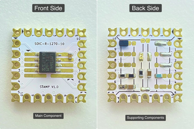
 Stamp solves this by offering reusable template boards with commonly used SMD footprints. You place the main component on the front and the supporting components on the back. Many complete circuits, such as buck converters, sensor blocks, microcontrollers, and so on, can fit on a single 17.8 × 17.8 mm board.
Most Stamps feature custom castellated holes, designed for side-by-side or right-angle edge connections, enabling a modular, reconfigurable approach to circuit building. The plan is to make the designs fully open source, so that others can build or adapt them. Although many PCB manufacturers might not have the facilities to make the special castellated edges which are available on some Stamps.
Dave Jones from the EEVblog covered the Stamp on one of his recent Mailbag videos, which you can check out below. This isn’t the first time we’ve seen somebody promise to reinvent the breadboard, but we do appreciate the simplicity of this approach.
Continue reading “Stamp: Modular Breakout Boards For SMD Prototyping” →