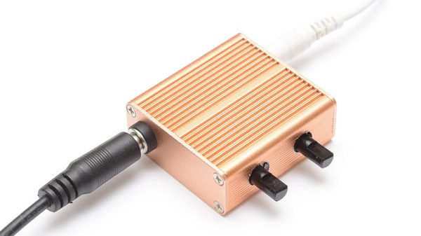
When you need a continuity tester at the bench, what do you reach for? Probably your multimeter, right? It may surprise you to know that the continuity tester in the meter isn’t all that sensitive, even if it’s the yellow expensive kind. [Leo]’s will beep even if there is 50Ω of resistance in the line.
Disgusted by modern commercial testers, [Leo] set out to make the ideal continuity tester in the spirit of old school tools that do one thing and do it really well. It had to be simple to use, always ready to go, and capable of measuring continuity at 5Ω or less resistance (video, embedded below).
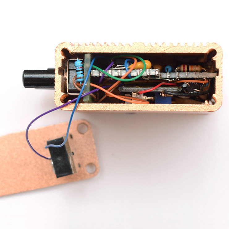
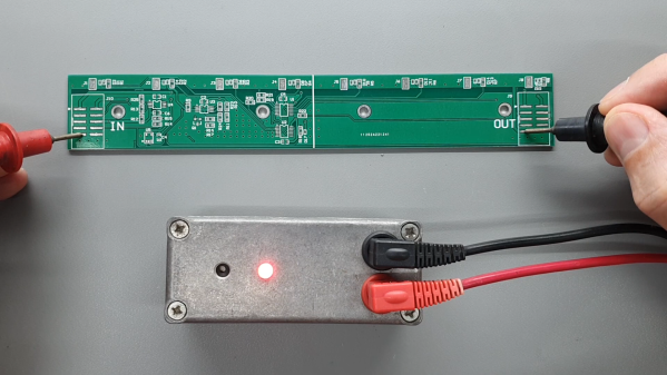
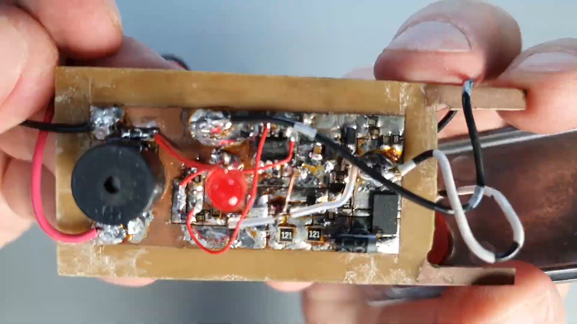 There’s no power switch or even labels, because it doesn’t need any. Just put the probes where you want ’em, and it either beeps and lights the LED or it doesn’t. It looks simple, but inside that blast-resistant enclosure are lots of cool features that certainly make it seem like the ideal tester to us.
Our favorite has to be the transient blocking unit that works like a little circuit breaker. They’re used to protect circuits from lighting and electrostatic discharge by way of depletion-mode MOSFETs and switches to protected mode in under a microsecond. Watch [Leo] build this workbench necessity and then abuse test it with mains power after the break.
Making your own tools, however simple or complex is a great experience. If you want to up your speedy prototyping game, [Leo]’s got you covered there with a special scratching tool for hand-scribing copper PCBs. Continue reading “Build An Everlasting Continuity Tester”