The central solenoid taking shape in the ITER assembly hall.

What’s Sixty Feet Across And Superconducting?

What’s sixty feet (18.29 meters for the rest of the world) across and superconducting? The International Thermonuclear Experimental Reactor (ITER), and probably not much else.

The last parts of the central solenoid assembly have finally made their way to France from the United States, making both a milestone in the slow development of the world’s largest tokamak, and a reminder that despite the current international turmoil, we really can work together, even if we can’t agree on the units to do it in.

A cutaway diagram of the ITER tokamak showing the central solenoid
The central solenoid is in the “doughnut hole” of the tokamak in this cutaway diagram. Image: US ITER.

The central solenoid is 4.13 m across (that’s 13′ 7″ for burger enthusiasts) sits at the hole of the “doughnut” of the toroidal reactor. It is made up of six modules, each weighing 110 t (the weight of 44 Ford F-150 pickup trucks), stacked to a total height of 59 ft (that’s 18 m, if you prefer). Four of the six modules have been installed on-site, and the other two will be in place by the end of this year.

Each module was produced ITER by US, using superconducting material produced by ITER Japan, before being shipped for installation at the main ITER site in France — all to build a reactor based on a design from the Soviet Union. It doesn’t get much more international than this!

This magnet is, well, central to the functioning of a tokamak. Indeed, the presence of a central solenoid is one of the defining features of this type, compared to other toroidal rectors (like the earlier stellarator or spheromak). The central solenoid provides a strong magnetic field (in ITER, 13.1 T) that is key to confining and stabilizing the plasma in a tokamak, and inducing the 15 MA current that keeps the plasma going.

When it is eventually finished (now scheduled for initial operations in 2035) ITER aims to produce 500 MW of thermal power from 50 MW of input heating power via a deuterium-tritium fusion reaction. You can follow all news about the project here.

While a tokamak isn’t likely something you can hack together in your back yard, there’s always the Farnsworth Fusor, which you can even built to fit on your desk.

PoX: Super-Fast Graphene-Based Flash Memory

Recently a team at Fudan University claimed to have developed a picosecond-level Flash memory device (called ‘PoX’) that has an access time of a mere 400 picoseconds. This is significantly faster than the millisecond level access times of NAND Flash memory, and more in the ballpark of DRAM, while still being non-volatile. Details on the device technology were published in Nature.

In the paper by [Yutong Xing] et al. they describe the memory device as using a two-dimensional Dirac graphene-channel Flash memory structure, with hot carrier injection for both electron and hole injection, meaning that it is capable of both writing and erasing. Dirac graphene refers to the unusual electron transport properties of typical monolayer graphene sheets.

Demonstrated was a write speed of 400 picoseconds, non-volatile storage and a 5.5 × 10⁶ cycle endurance with a programming voltage of 5 V. It are the unique properties of a Dirac material like graphene that allow these writes to occur significantly faster than in a typical silicon transistor device.

What is still unknown is how well this technology scales, its power usage, durability and manufacturability.

Preventing Galvanic Corrosion In Water Cooling Loops

Water is an excellent coolant, but the flip side is that it is also an excellent solvent. This, in short, is why any water cooling loop is also a prime candidate for an interesting introduction to the galvanic metal series, resulting in severe corrosion that commences immediately. In a recent video by [der8aer], this issue is demonstrated using a GPU cold plate. The part is made out of nickel-plated copper and features many small channels to increase surface area with the coolant.

The surface analysis of the sample cold plate after a brief exposure to distilled water, showing the deposited copper atoms. (Credit: der8auer, YouTube)
The surface analysis of the sample cold plate after a brief exposure to distilled water shows the deposited copper atoms. (Credit: der8auer, YouTube)

Theoretically, if one were to use distilled water in a coolant loop that contains a single type of metal (like copper), there would be no issue. As [der8auer] points out, fittings, radiators, and the cooling block are nearly always made of various metals and alloys like brass, for example. This thus creates the setup for galvanic corrosion, whereby one metal acts as the anode and the other as a cathode. While this is desirable in batteries, for a cooling loop, this means that the water strips metal ions off the anode and deposits them on the cathode metal.

The nickel-plated cold plate should be immune to this if the plating were perfect. However, as demonstrated in the video, even a brief exposure to distilled water at 60°C induced strong galvanic corrosion. Analysis in an SEM showed that the imperfect nickel plating allowed copper ions to be dissolved into the water before being deposited on top of the nickel (cathode). In a comparison with another sample that had a coolant with corrosion inhibitor (DP Ultra) used, no such corrosion was observed, even after much longer exposure.

This DP Ultra coolant is mostly distilled water but has glycol added. The glycol improves the pH and coats surfaces to prevent galvanic corrosion. The other element is benzotriazole, which provides similar benefits. Of course, each corrosion inhibitor targets a specific environment, and there is also the issue with organic films forming, which may require biocides to be added. As usual, water cooling has more subtlety than you’d expect.

Continue reading “Preventing Galvanic Corrosion In Water Cooling Loops”

The TMSR-LF1 building seen from the sky. (Credit: SINAP)

China’s TMSR-LF1 Molten Salt Thorium Reactor Begins Live Refueling Operations

Although uranium-235 is the typical fuel for commercial fission reactors on account of it being fissile, it’s relatively rare relative to the fertile U-238 and thorium (Th-232). Using either of these fertile isotopes to breed new fuel from is thus an attractive proposition. Despite this, only India and China have a strong focus on using Th-232 for reactors, the former using breeders (Th-232 to U-233) to create fertile uranium fuel. China has demonstrated its approach — including refueling a live reactor — using a fourth-generation molten salt reactor.

Continue reading “China’s TMSR-LF1 Molten Salt Thorium Reactor Begins Live Refueling Operations”

A nuclear coolant tower dwarfs other buildings in the area.

They Hacked A Nuclear Power Plant! Whoops! Don’t Make A Sound!

What do you do with an unused nuclear reactor project? In Washington, one of them was hacked to remove sound, all in the name of science.

In 1977, a little way outside of Seattle, Washington Nuclear Projects 3 and 5 (WNP-3 and WNP-5) were started as part of Washington Public Power Supply System (WPPSS, pronounced “whoops”). They ran over budget, and in the 80s they were mothballed even though WNP-3 was nearly complete.

Continue reading “They Hacked A Nuclear Power Plant! Whoops! Don’t Make A Sound!”

An electron microscope image of the aluminum alloy from the study.

D20-shaped Quasicrystal Makes High-Strength Alloy Printable

When is a crystal not a crystal? When it’s a quasi-crystal, a paradoxical form of metal recently found in some 3D printed metal alloys by [A.D. Iams et al] at the American National Institute for Standards and Technology (NIST).

As you might remember from chemistry class, crystals are made up of blocks of atoms (usually called ‘unit cells’) that fit together in perfect repetition — baring dislocations, cracks, impurities, or anything else that might throw off a theoretically perfect crystal structure. There are only so many ways to tessellate atoms in 3D space; 230 of them, to be precise. A quasicrystal isn’t any of them. Rather than repeat endlessly in 3D space, a quasicrystal never repeats perfectly, like a 3D dimensional Penrose tile. The discovery of quasicrystals dates back to the 1980s, and was awarded a noble prize in 2011.

Penrose tiling of thick and thin rhombi
Penrose tiling– the pattern never repeats perfectly. Quasicrystals do this in 3D. (Image by Inductiveload, Public Domain)

Quasicrystals aren’t exactly common in nature, so how does 3D printing come into this? Well, it turns out that, quite accidentally, a particular Aluminum-Zirconium alloy was forming small zones of quasicrystals (the black spots in the image above) when used in powder bed fusion printing. Other high strength-alloys tended to be very prone to cracking, to the point of unusability, and this Al-Zr alloy, discovered in 2017, was the first of its class.

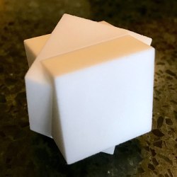
You might imagine that the non-regular structure of a quasicrystal wouldn’t propagate cracks as easily as a regular crystal structure, and you would be right! The NIST researchers obviously wanted to investigate why the printable alloy had the properties it does. When their crystallographic analysis showed not only five-fold, but also three-fold and two-fold rotational symmetry when examined from different angles, the researchers realized they had a quasicrystal on their hands. The unit cell is in the form of a 20-sided icosahedron, providing the penrose-style tiling that keeps the alloy from cracking.

You might say the original team that developed the alloy rolled a nat-20 on their crafting skill. Now that we understand why it works, this research opens up the doors for other metallic quasi-crystals to be developed on purpose, in aluminum and perhaps other alloys.

We’ve written about 3D metal printers before, and highlighted a DIY-able plastic SLS kit, but the high-power powder-bed systems needed for aluminum aren’t often found in makerspaces. If you’re building one or know someone who is, be sure to let us know.

Budget Schlieren Imaging Setup Uses 3D Printing To Reveal The Unseen

We’re suckers here for projects that let you see the unseeable, and [Ayden Wardell Aerospace] provides that on a budget with their $30 Schlieren Imaging Setup. The unseeable in question is differences in air density– or, more precisely, differences in the refractive index of the fluid the imaging set up makes use of, in this case air. Think of how you can see waves of “heat” on a warm day– that’s lower-density hot air refracting light as it rises. Schlieren photography takes advantage of this, allowing to analyze fluid flows– for example, the mach cones in a DIY rocket nozzle, which is what got [Ayden Wardell Aerospace] interested in the technique.

Shock diamonds from a homemade rocket nozzle imaged by this setup.
Examining exhaust makes this a useful tool for [Aerospace].
This is a ‘classic’ mirror-and-lamp Schlieren set up.  You put the system you wish to film near the focal plane of a spherical mirror, and camera and light source out at twice the focal distance. Rays deflected by changes in refractive index miss the camera– usually one places a razor blade precisely to block them, but [Ayden] found that when using a smart phone that was unnecessary, which shocked this author.

While it is possible that [Ayden Wardell Aerospace] has technically constructed a shadowgraph, they claim that carefully positioning the smartphone allows the sharp edge of the case to replace the razor blade. A shadowgraph, which shows the second derivative of density, is a perfectly valid technique for flow visualization, and is superior to Schlieren photography in some circumstances– when looking at shock waves, for example.

Regardless, the great thing about this project is that [Ayden Wardell Aerospace] provides us with STLs for the mirror and smartphone mounting, as well as providing a BOM and a clear instructional video. Rather than arguing in the comments if this is “truly” Schlieren imaging, grab a mirror, extrude some filament, and test it for yourself!

There are many ways to do Schlieren images. We’ve highighted background-oriented techniques, and seen how to do it with a moiré pattern, or even a selfie stick. Still, this is the first time 3D printing has gotten involved and the build video below is quick and worth watching for those sweet, sweet Schlieren images. Continue reading “Budget Schlieren Imaging Setup Uses 3D Printing To Reveal The Unseen”