PS5 Goes On Slim-Fast

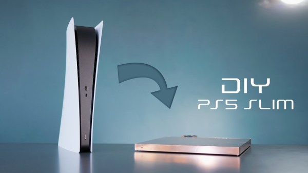
For the past few decades, most console makers have first come out with a large flagship model, and then a few years later, released a smaller, more compact slim edition. Not content to wait for it, [Matt] at DIY Perks made his own PS5 Slim, and the results are awe-inspiring.

Generally, slim editions are made by lowering the TDP of the chip under the hood. A lower power draw means less cooling is needed, a smaller power supply can be used, and a design that is overall easier to manage. Unfortunately, [Matt] had none of these benefits and instead had to contend with the full 180 W that the AMD CPU inside the PlayStation can draw.

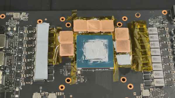
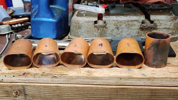
Taking apart the console left him with the main board that was quite thick as it had heat pipes on both sides. His first thought was water cooling as it can rapidly move the heat needed, but even with right-angle fittings, it didn’t fit within the ambitious thickness goal he had set for himself of less than 2 cm (about 3/4″). To do that, [Matt] had to fabricate a copper water block from three sheets of copper. The first one connects to the motherboard via standoffs and has cut-outs for various connectors and parts. The middle layer has a channel through which water can flow, and the last layer seals it together.

With the three layers together, he soldered them in a toaster oven repurposed as a reflow oven. Cleverly, he used silicone grease to prevent solder from getting into areas he didn’t want, like the fins in the CPU block. Luckily, the grease dissolved in alcohol, and after flushing the chamber, he had a solid copper, water-tight, custom loop.  However, on his road to glory, [Matt] ran into a snag. He accidentally covered the intake vent on the radiator, and the PS5 overheated, killing it. With a fried mainboard and a project almost on the cusp of completion, he resorted to using the PS5 he had received for B-roll.

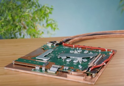
Last-minute motherboard swap aside, the final project is gorgeous. The polished exterior and sheer thinness of it are striking. [Matt] has already disguised his PS5 before and after this, we’re not quite sure where he could possibly take it next. But we’re excited to find out.

Continue reading “PS5 Goes On Slim-Fast”

Turning Scrap Copper Into Beautiful Copper Acetate Crystals

Crystals, at least those hawked by new-age practitioners for their healing or restorative powers, will probably get a well-deserved eye roll from most of the folks around here. That said, there’s no denying that crystals do hold sway over us with the almost magical power of their beauty, as with these home-grown copper acetate crystals.

The recipe for these lovely giant crystals that [Chase Lean] shares is almost too simple — just scrap copper, vinegar, and a bit of hydrogen peroxide — and just the over-the-counter strength versions of those last two. The process begins with making a saturated solution of copper acetate by dissolving the scrap copper bits in the vinegar and peroxide for a couple of days. The solution is concentrated by evaporation until copper acetate crystals start to form. Suspend a seed crystal in the saturated solution, and patience will eventually reward you with a huge, shiny blue-black crystal. [Chase] also shares tips for growing crystal clusters, which have a beauty of their own, as do dehydrated copper acetate crystals, with their milky bluish appearance.

Is there any use for these crystals? Probably not, other than their beauty and the whole coolness factor of watching nature buck its own “no straight lines” rule. And you’ll no doubt remember [Chase]’s Zelda-esque potassium ferrioxalate crystals, or even when he turned common table salt into perfect crystal cubes.

Copper Modding Helps Cool A Toasty GPU

[DandyWorks] had an NVIDIA RTX 3070 Ti GPU, and found it was running incredibly hot, with the card’s memory hitting temperatures of 110 °C. He decided to try “copper modding” to solve the problem, and made some impressive improvements along the way.

Copper modding is where small copper shims are used to connect hot chips on the GPU to the heatsink more effectively than the standard thermal pads used by the manufacturer. Copper has much better thermal conductivity than thermal pads, and thus can help improve cooling of components when used in this fashion.

With the GPU carefully disassembled, [DandyWorks] notes the design uses a sub-heatsink specifically for the memory chips. He then sets about removing the thermal pads from the chips with isopropyl alcohol to help. They’re replaced with copper shims of a precise thickness, with a thin layer of thermal paste to ensure good heat flow. [DandyWorks] also shields all surrounding parts of the board with Kapton tape to avoid shorts if the copper shims happen to shift at any point.

Running the same hashing operation, the GPU now operates with its memory at a much cooler temperature of just 64 °C. [DandyWorks] ran the test for hours and temperatures didn’t climb beyond there. It’s evidence that the copper shims do a far better job of conducting the heat out of the memory chips versus the stock thermal pad setup.

We’ve seen some other interesting mods in this vein before, such as CPU die lapping for better thermal performance. Video after the break.

Continue reading “Copper Modding Helps Cool A Toasty GPU”

Mining And Refining: Copper, The Metal That Built Technology

It’s hard to reckon exactly when in history humans became a technological species. Part of that is because the definition of technology is somewhat subjective; if you think making a stick pointy enough to grub roots from the dirt or to poke enough holes in an animal to convince it to let you eat it is technology, then our engineered world goes back a long, long way indeed.

But something about pointy sticks just doesn’t seem transformative enough, in the sense of fundamentally changing a naturally occurring material, to really count as a technological line in the sand. To cross that line, it really seems like the use of metals should be part of the package. Even if that’s the case, our technological history still goes pretty far back. And copper ends up being one of the metals that started it all, about 11,000 years ago, when our ancestors discovered natural deposits of the soft, reddish metal and began learning how to fashion it into the tools and implements that lifted us out of the Stone Age.

Our world literally cannot run without copper, forming as it does not only the electric-motor muscles of civilization, but also the wires and cables that form the power and data grids that stitch us together. Ironically, we are just as dependent on copper now as we were when it was the only metal we could make tools from, and perhaps more so. We’ll take a look at what’s involved in extracting and purifying copper, and see how the methods we today use are not entirely different from those developed over seven millennia ago.

Continue reading “Mining And Refining: Copper, The Metal That Built Technology”

PCB internal bodge

PCB Microsurgery Puts The Bodges Inside The Board

We all make mistakes, and there’s no shame in having to bodge a printed circuit board to fix a mistake. Most of us are content with cutting a trace or two with an Xacto or adding a bit of jumper wire to make the circuit work. Very few of us, however, will decide to literally do our bodges inside the PCB itself.

The story is that [Andrew Zonenberg] was asked to pitch in debugging some incredibly small PCBs for a prototype dev board that plugs directly into a USB jack. The six-layer boards are very dense, with a forest of blind vias. The Twitter thread details the debugging process, which ended up finding a blind via on layer two shorted to a power rail, and another via shorted to ground. It also has some beautiful shots of [Andrew]’s “mechanical tomography” method of visualizing layers by slowly grinding down the surface of the board.

[Andrew] has only tackled one of the bodges at the time of writing, but it has to be seen to be believed. It started with milling away the PCB to get access to the blind via using a ridiculously small end mill. The cavity [Andrew] milled ended up being only about 480 μm by 600 μm and only went partially through a 0.8-mm thick board, but it was enough to resolve the internal short and add an internal bodge to fix a trace that was damaged during milling. The cavity was then filled up with epoxy resin to stabilize the repair.

This kind of debugging and repair skill just boggles the mind. It reminds us a bit of these internal chip-soldering repairs, but taken to another level entirely. We can’t wait to see what the second repair looks like, and whether the prototype for this dev board can be salvaged.

Thanks to [esclear] for the heads up on this one.

Copper tubes formed by 3D printed press dies

Can 3D Printed Press Tools Produce Repeatable Parts?

When we think of using a press to form metal we think of large stamps with custom made metal dies under unimaginable hydraulic pressure. It’s unlikely we’d e think of anything 3D printed. And in a commercial environment we’d be right. But your average garage hacker is far more likely to have access to a bench vise and a 3D printer. It’s in this context that [The Shipping Container Garage] has spent considerable time, effort, and money perfecting a process for pressing copper parts with 3D printed dies, which you can watch below the break.

In the quest to make a custom intake manifold for his project car, [The Shipping Container Garage] first made 3D printed jigs for cutting out a manifold flange that bolts to the cylinder head. It’s a process he calls Analog CNC, as all the cutting is done by hand.

Buoyed by his success, he proceeded with the next step: making manifold runners. His metal of choice was copper. While softer than many metals such as steel, he found it too hard. In the video, he describes his method for annealing the copper. Once cooled, two 3D printed dies are pressed into the copper tubes to progressively shape them. Watch the video to find out one of the neatest details of the die itself: how he gets it out!

Of course no matter how clever this all is, it’s useless if it produces poor results. And that’s where the most astounding part of the build is: The parts are all the same within 0.006 inches (0.15mm) of each other, and the parts fit the manifold flange they were made for. Additionally, the die can be used for the duration of the project at hand. For low volume production, this appears to be a viable method. It’ll be interesting to see what others do to iterate these processes to even more advanced stages.

You may also like to see 3D printing used in leather working and in jigs for beautiful circuit sculptures. A big thanks to [JapanFan] for the tip! If you have your own pressing hacks to share, let us know via the Tip Line!

Continue reading “Can 3D Printed Press Tools Produce Repeatable Parts?”

The Coming Copper Shortage: Aluminium Or Carbon Nanotubes To The Rescue?

The use of aluminium in wiring is unlikely to bring a smile to the face of anyone who has had to deal with it in a 1960s, or early 1970s-era house. The causes behind the fires and other accidents were myriad, including failure to deal with the higher thermal expansion of aluminium, the electrically insulating nature of aluminium oxide, and the general brittleness of aluminium when twisted.

Yet while copper is superior to aluminium in terms of electrical conductivity and ease of installation, copper prices have skyrocketed since the 1970s, and are on the verge of taking off to the moon. A big part of the reason is the increased use of copper in everything from electronics and electrical motors to generators, driven by large-scale deployment of wind turbines and electrical vehicles.

As the world moves to massively expand the use of electrical cars and installation of wind turbines, copper demand is predicted to outstrip current copper supply. With aluminium likely to make a big return as a result, it’s worth taking a look at modern-day aluminium-based wiring, including copper-clad aluminium and the use of carbon-based replacements. Continue reading “The Coming Copper Shortage: Aluminium Or Carbon Nanotubes To The Rescue?”