The 6502 is the classic CPU. This chip is found in the original Apple, Apple II, PET, Commodore 64, BBC Micro, Atari 2600, and 800, the original Nintendo Entertainment System, Tamagotchis, and Bender Bending Rodriguez. This was the chip that started the microcomputer revolution, and holds a special place in the heart of every nerd and technophile. The 6502 is also possibly the most studied processor, with die shots of polysilicon and metal found in VLSI textbooks and numerous simulators available online.
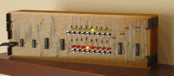
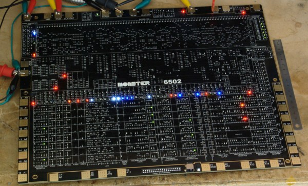
The only thing we haven’t seen, until now, is a version of the 6502 built out of discrete transistors. That’s what [Eric Schlaepfer] has been working on over the past year. It’s huge – 12 inches by 15 inches – has over four thousand individual components, and so far, this thing works. It’s not completely tested, but the preliminary results look good.
The MOnSter 6502 began as a thought experiment between [Eric] and [Windell Oskay], the guy behind Evil Mad Scientist and creator of the discrete 555 and dis-integrated 741 kits. After realizing that a few thousand transistors could fit on a single panel, [Eric] grabbed the netlist of the 6502 from Visual6502.org. With the help of several scripts, and placing 4,304 components into a board design, the 6502 was made dis-integrated. If you’re building a CPU made out of discrete components, it only makes sense to add a bunch of LEDs, so [Eric] threw a few of these on the data and address lines.
This is the NMOS version of the 6502, not the later, improved CMOS version. As such, this version of the 6502 doesn’t have all the instructions some programs would expect. The NMOS version is slower, more prone to noise, and is not a static CPU.
So far, the CPU is not completely tested and [eric] doesn’t expect it to run faster than a few hundred kilohertz, anyway. That means this gigantic CPU can’t be dropped into an Apple II or commodore; these computers need a CPU to run at a specific speed. It will, however, work in a custom development board.
Will the gigantic 6502 ever be for sale? That’s undetermined, but given the interest this project will receive it’s a foregone conclusion.
Correction: [Eric] designed the 555 and 741 kits