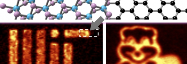
An ordinary integrated circuit is made of layers of material. Typically a layer is made from some material (like silicon dioxide, polysilicon, copper, or aluminum). Sometimes a process will modify parts of a layer (for example, using ion implantation to dope regions of silicon). Other times, some part of the layer will be cut away using a photolithography process.
Researchers at MIT have a new technique that allows super thin layers (1-3 atoms thick) and–even more importantly–enables you to use two materials in the same layer. They report that they have built all the basic components required to create a computer using the technique.
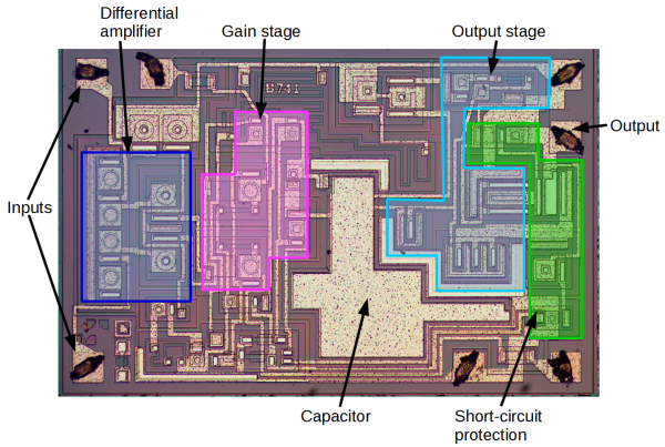
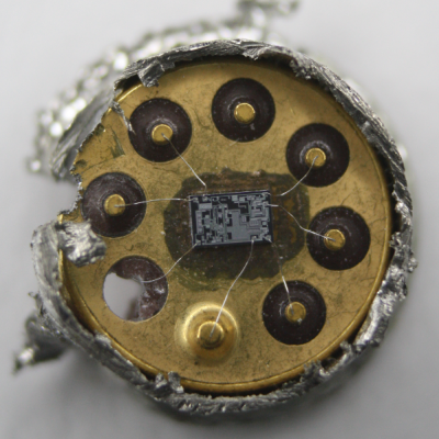 Rather than risk the boiling acid method commonly used to decap epoxy-potted ICs, [Ken] wisely chose a TO-99 can format to attack with a hacksaw. With the die laid bare for his microscope, he was able to locate all the major components and show how each is implemented in silicon. Particularly fascinating is the difference between the construction of NPN and PNP transistors, and the concept of “current mirrors” as constant current sources. And he even whipped up a handy interactive chip viewer – click on something in the die image and find out which component it is on the 741 schematic. Very nice.