TL084 die blocks

Ken Shirriff Found Butterflies In His Op-Amp

In 1976, Texas Instruments came out with the TL084, a four JFET op-amp IC each with similar circuitry to Fairchild’s very popular single op-amp 741. But even though the 741 has been covered in detailed, when [Ken Shirriff] focused his microscope on a TL084, he found some very interesting things.

JFETs on the TL084 op-amp

To avoid using acid to get at the die, he instead found a ceramic packaged TL084 and pried off the cover. The first things he saw were four stabilizing capacitors, by far the largest structures on the die and visible to the naked eye.

When he peered into his microscope he next saw butterfly shapes which turned out to be pairs of input JFETs. The wide strips are the gates and the narrower strip surrounded by each gate is the source. The drain is the narrow strip surrounding each gate. Why arrange four JFETs like this? It’s possible to have temperature gradients in the IC, one side being hotter than the other. These gradients can affect the JFET’s characteristics, unbalancing the inputs. Look closely at the way the JFETs are connected and you’ll see that the top-left one is connected to the bottom-right one, and similarly for the other two. This diagonal cross-connecting cancels out any negative effects.

[Ken’s] analysis in his article doesn’t stop there though. Not only does he talk more about these JFETs but he goes over the rest of the die too. It’s well worth the read, as is his write-up about the 741 which we’ve also covered.

More Details On That First Home-Made Lithographically Produced IC

A few days ago we brought you news of [Sam Zeloof]’s amazing achievement, of creating the first home-made lithographically produced integrated circuit. It was a modest enough design in a simple pair of differential amplifiers and all we had to go on was a Twitter announcement, but it promised a more complete write-up to follow. We’re pleased to note that the write-up has arrived, and we can have a look at some of the details of just how he managed to produce an IC in his garage. He’s even given it a part number, the Zeloof Z1.

For ease of manufacture he’s opted for a PMOS process, and he is using four masks which he lists as the active/doped area, gate oxide, contact window, and top metal. He takes us through 66 different processes that he performs over the twelve hours of a full production run, with comprehensive descriptions that make for a fascinating run-down of semiconductor manufacture for those of us who will never build a chip of our own but are still interested to learn how it is done. The chip’s oblong dimensions are dictated by the constraints of an off-the-shelf Kyocera ceramic chip carrier, though without a wire bonding machine he’s unable to do any more than test it with probes.

You can read our reporting of his first announcement, but don’t go away thinking that will be all. We’re certain [Sam] will be back with more devices, and can’t wait to see the Z2.

First Lithographically Produced Home Made IC Announced

It is now six decades since the first prototypes of practical integrated circuits were produced. We are used to other technological inventions from the 1950s having passed down the food chain to the point at which they no longer require the budget of a huge company or a national government to achieve, but somehow producing an integrated circuit has remained out of reach. It’s the preserve of the Big Boys, move on, there’s nothing to see here.

Happily for us there exists a dedicated band of experimenters keen to break that six-decade dearth of home-made ICs. And now one of them, [Sam Zeloof], has made an announcement on Twitter that he has succeeded in making a dual differential amplifier IC using a fully lithographic process in his lab. We’ve seen [Jeri Ellsworth] create transistors and integrated circuits a few years ago and he is at pains to credit her work, but her interconnects were not created lithographically, instead being created with conductive epoxy.

For now, all we have is a Twitter announcement, a promise of a write-up to come, and full details of the lead-up to this momentous event on [Sam]’s blog. He describes both UV lithography using a converted DLP projector and electron beam lithography using his electron microscope, as well as sputtering to deposit aluminium for on-chip interconnects. We’ve had an eye on his work for a while, though his progress has been impressively quick given that he only started amassing everything in 2016. We look forward to greater things from this particular garage.

Deconstructing A Simple Op-Amp

Maybe you are familiar with the op-amp as an extremely versatile component, and you know how to quickly construct a huge variety of circuits with one. Maybe you even have a favorite op-amp or two for different applications, covering many possible niches. Standard circuits such as an inverting amplifier are your bread and butter, and the formula gain=-Rf/Ri is tattooed on your forearm.

But you can know how to use op-amps without really knowing how they work. Have you ever peered under the hood of an op-amp to find out what’s going on in there? Would you like to? Let’s take a simple device and examine it, piece by piece.

Continue reading “Deconstructing A Simple Op-Amp”

How The Integrated Circuit Came To Be

As the saying goes, hindsight is 20/20. It may surprise you that the microchip that we all know and love today was far from an obvious idea. Some of the paths that were being explored back then to cram more components into a smaller area seem odd now. But who hasn’t experienced hindsight of that sort, even on our own bench tops.

Let’s start the story of the microchip like any good engineering challenge should be started, by diving into the problem that existed at the time with the skyrocketing complexity of computing machines.

Continue reading “How The Integrated Circuit Came To Be”

Project 54/74 Maps Out Logic ICs

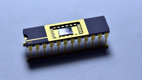
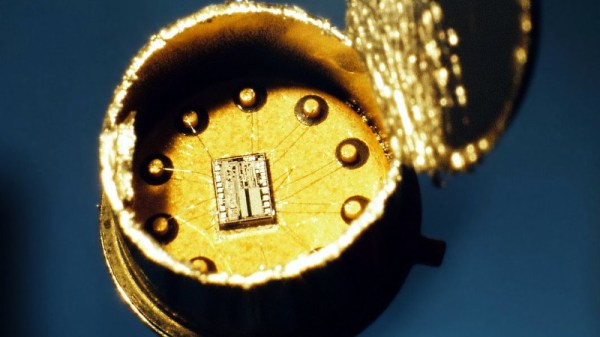
Integrated circuits are a fundamental part of almost all modern electronics, yet they closely resemble the proverbial “black box” – we may understand the inputs and outputs, but how many of us truly understand what goes on inside? Over the years, the process of decapping ICs has become popular – the removal of the package to enable peeping eyes to glimpse the mysteries inside. It’s an art that requires mastery of chemistry, microscopy and photography on top of the usual physics skills needed to understand electronics. Done properly, it allows an astute mind to reverse engineer the workings of the silicon inside.

There are many out there publishing images of chips they’ve decapped, but [Robert Baruch] wants more. Namely, [Robert] seeks to create a database of die images of all 5400 and 7400 series logic chips – the eponymous Project 54/74.

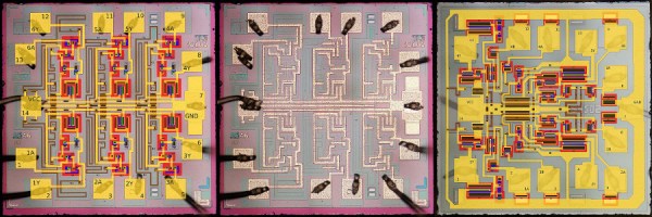
These chips are the basic building blocks of digital logic – NAND gates, inverters, shift registers, decade counters and more. You can build a CPU with this stuff. These days, you may not be using these chips as often in a production context, but those of you with EE degrees will likely have toyed around a few of these in your early logic classes.

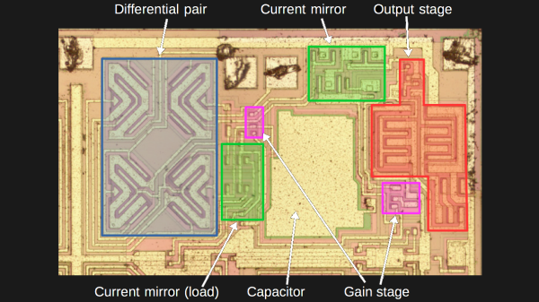
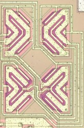
There’s only a handful of images up so far, but they’re of excellent quality, and they’re also annotated. This is a great aid if you’re trying to get to grips with the vagaries of chip design. [Robert] is putting in the hard yards to image as many variations of every chip as possible. There’s also the possibility of comparing the same chip for differences between manufacturers. We particularly like this project, as all too often manufacturing techniques and technologies are lost and forgotten as the march of progress continues on. It looks like it’s going to become a great resource for those looking to learn more about integrated circuit design and manufacture!

Super Thin ICs Are Coming

An ordinary integrated circuit is made of layers of material. Typically a layer is made from some material (like silicon dioxide, polysilicon, copper, or aluminum). Sometimes a process will modify parts of a layer (for example, using ion implantation to dope regions of silicon). Other times, some part of the layer will be cut away using a photolithography process.

Researchers at MIT have a new technique that allows super thin layers (1-3 atoms thick) and–even more importantly–enables you to use two materials in the same layer. They report that they have built all the basic components required to create a computer using the technique.

Continue reading “Super Thin ICs Are Coming”