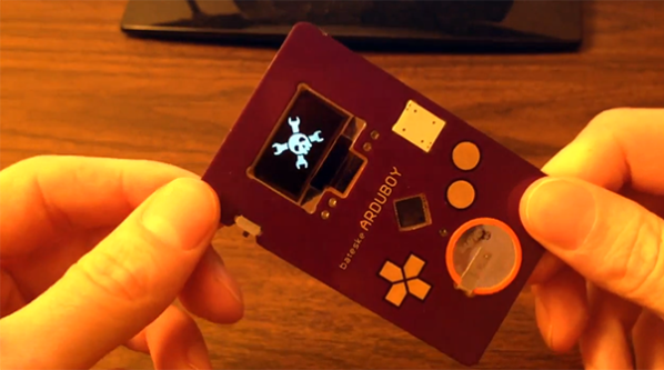
Think you’ve seen every possible type of Arduino based hand held video game? [Kevin] managed to coax something new out of the theme with a very clever credit card sized console that uses some very interesting construction techniques.
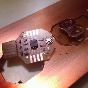
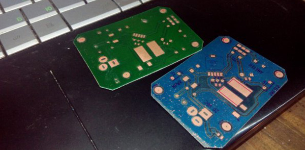
The inspiration for this project began when [Kevin] dropped an SMD resistor into a drill hole on a PCB. This resistor fell right through the hole, giving him the idea creating a PCB with milled cutouts made to fit SMD components. With a little experimentation, [Kevin] found he could fit a TQFP32 ATMega328p – the same microcontroller in the Arduino – in a custom square cutout. The rest of the components including a CR2016 battery and OLED display use the same trick.
The rest of the design involved taking Adafruit and Sparkfun breakout boards, and modifying the individual circuits until something broke. Then, off to Eagle to create a PCB.
[Kevin]’s experiment in extremely unusual PCB design worked, resulting in a credit-card sized “Game Boy” that’s only 1.6 millimeters thick. The controls are capacitive touch sensors and he already has an easter egg hidden in the code; enter the Konami code and the Hackaday logo pops up to the tune of [Rick Astley]’s magnum opus.
Now [Kevin] is in a bit of a bind. He’d like to take this prototype and turn it into a crowd sourced campaign. In our opinion, this “Game Boy in a wallet” would probably do well on a site like Tindie, but any sort of large scale manufacturing is going to be a rather large pain. If you have any wishes, advice, of complaints for [Kevin] he’s got a few links at the bottom of his project page.