Hackaday Links: October 18, 2012

Capacitive touch plants

Here’s a proof of concept for using plants as a capacitive touch sensor. The sensor is simply a hunk of double-sided copper clad board attached to a microcontroller. But it seems to be able to sense what part of the plant is being touched. [Thanks Fabien]

Adding wireless charging to a Nokia N900

This hack is quite common, but it’s still fun to see what hardware is being outfitted with an inductive charger. This time it’s a Nokia N900 that’s ditching the charging cables.

Wii carrying suitcase from a plastic tackle box

This Wii carrying case (translated) looks great and cost just a few bucks. It started as a tackle box for carrying around your fishing lures. But a bit of creative cutting and there’s a place for everything.

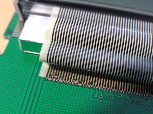
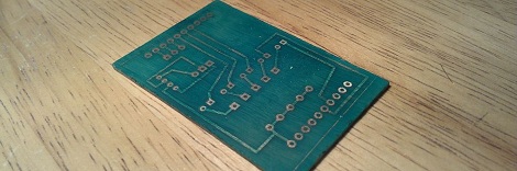
Browser based schematic and board layout

There’s a new kid on the block when it comes to circuit design. Circuits.io offers in-brower schematic design and board artwork layout. [Thanks ADIDAIllinie (and a few others)]

Bender-o-lantern

Halloween rapidly approaches and we hope that [Tim’s] carving of Bender in a pumpkin will inspire you to send in your own Halloween projects.

How To Repair A Ribbon Cable Connection On Consumer Electronics

It’s not uncommon in cheaper devices to find a ribbon cable soldered directly to the circuit board like the one pictured above. Using a connector would have been a much more resilient approach, but adding parts adds cost. If you take a close look you’ll see things aren’t looking so great anymore. [Chaotic and Random] pulled this board out of his VW Camper Van. Rather than buy an expensive replacement part, he shows us how to repair a soldered ribbon wire connection.

This repair is rather invasive and he suggests trying some hot-air rework (possibly using a heat gun) to fix up any misbehaving connections. But if that has failed it’s time for the knife. The first step is to  cut the ribbon so that the LCD can be removed from the board. From there he peels the remaining scrap off ribbon of the pads. This makes us cringe as it could lift traces from the PCB, but he was gentle enough to avoid it. Now comes the time to start reassembling. After thoroughly cleaning the pads the ribbon is cut straight and resoldered. The trick is to flow the solder without melting the ribbon. He uses tin foil to cover the tip and cools it on a moist sponge just before reflowing solder.

It sounds like more art than science. But when the only alternative is to spend hundreds on a new part it may be worth a try.

Integrating A Power Bus Into A Quadcopter Frame

When working on flying vehicles weight is always a consideration. [Brendin] found a way to get rid of a wiring harness on his quadcopter, simplifying the assembly while lightening the load. He did it by incorporating the power bus into the frame of the vehicle.

He started with some copper clad board. Because the substrate is a structural component he didn’t want to use a CNC mill to do the etching as it also removes a bit more than just copper. After using the mill to cut out the shape and drill holes he coated the board with flat black paint. This acts as the etch resist, which he sent through a 50W laser engraver to remove the paint and expose the areas he wants to etch. After etching he removed the rest of the resist, and masked off his solder pads with small rectangles of electrical tape. This protects the solder pads from the truck bed liner paint he uses to insulate the copper. He says it works great and plans to use the technique on all future builds.

Etching Brass And Copper With The Etchinator

If you’re in to making your own PCBs at home, you know the trials of etching copper clad boards. It’s slow, even if you’re gently rocking your etch tank or even using an aquarium pump to agitate your etching solution. [cunning_fellow] over on Instructables has the solution to your etching problems, and can even produce printmaking plates, jewelry, photochemically machine small parts, and make small brass logos of your second favorite website.

The Etchinator is a spray etcher, so instead of submerging a copper clad board into a vat of ferric or cupric chloride, etching solution is sprayed onto the board. We’ve seen this technique before, but previous builds use pumps to spray the etching solution and cost a bundle. [cunning_fellow]’s Etchinator doesn’t used pumps; it’s driven by two cordless drill motors sucking up etching solution through a hollow tube.

The basic idea behind the build is sticking a vertical PVC pipe in a box with etching solution. Mount an impeller in the bottom of the tube, drill many small holes in the side of the tube, and spin it with a motor up top. The solution is sucked up the tube, sprayed out the sides, and falls back down into the reservoir. Put a masked off copper board in the tank and Bob’s your uncle.

Not only did [cunning_fellow] come up with an awesome PCB etching solution, but the same machine can be used for etching brass plate for printmaking, and even photoetching brass sheets for model planes, trains, and automobiles. The quality is really amazing; the Instructables robot above was etched out of 0.7 mm thick brass, with an etch depth of 0.35 mm with only 0.05 mm of undercut. A very awesome build that is already on our ‘to build’ project list.

Radio Built From The London Underground Map

We love it when PCB artwork is actually artwork. Here’s one example of a radio whose layout mimics the map of London’s subway system.

The build is for an exhibit at the London Design Museum. They have an artist in residence program which allowed Yuri Suzuki time and resources to undertake the project. He speaks briefly about the concepts behind it in the video after the break.

The top layer of copper, and silk screen was positioned to mirror the subway lines and stops on a traditional transportation map. Major components represent various transfer hubs. In this way he hopes the functioning of the circuit can be followed by a layman in the same way one would plan a trip across town.

This may be a bit more abstract than you’re willing to go with your own projects. But there are certainly other options to spicing you track layout.

Continue reading “Radio Built From The London Underground Map”

Put A Solder Mask On Those Homebrew PCBs

While making your own PCBs at home is one of the best marks of a competent builder, if you want to give your project a more professional vibe, you’re going to need to do better than bare copper traces on a piece of fiberglass. To help out his fellow makers, [Chris] sent in his Instructable on creating a solder mask for homemade circuit boards using a minimal amount of tools and materials easily sourced from the Internet.

[Chris]’ soldermasks are made from UV curing paints he found on eBay. Of course the traditional green paint is available, along with paints very similar to the Sparkfun red or Arduino blue soldermasks.

After brushing the soldermask paint onto his home-etched circuit board, [Chris] printed out the solder mask onto a piece of transparency film using a laser printer. This mask is vitally important if you ever plan to solder your board; by covering the pads you wish to solder, the paint won’t cure and can later be removed.

[Chris] cured his soldermask by leaving it in the sun for a half hour. After the paint was dry, he removed the excess paint covering the pads with a little bit of turpentine and some elbow grease.

While [Chris]’ paint had somewhat of an ugly matte finish, the soldermask does its job, protecting the PCB traces while leaving the pads uncovered and ready to solder.

Etching Your Own PCBs At Home

Etching your own PCBs from copper clad board is nothing new, but the ability to make your own circuit boards at home is so useful it should be part of every maker’s repertoire of skills. The folks over at Hub City Labs in Moncton, NB, Canada put together a workshop covering the basics of home PCB manufacturing, allowing any maker to put a circuit board in their hands in under an hour.

The process starts just like any PCB design – laying out traces, parts, and vias in a PCB designer such as Eagle. When making your own boards, it’s a good idea to make the traces and pads extra large; the folks at Hub City Labs follow the 50-50 rule: 50 mil wide traces with 50 mils of seperation.

The PCB design is printed out with a laser printer (in mirror mode) onto a piece of paper from a glossy magazine or inkjet photo paper. After the copper board is scrubbed to remove any oxidation or oils present, the design is laid face down on the copper and heated with a clothes iron or sent through a laminator.

After the laser printer toner is transferred to the copper, the recipe calls for etching the board with a solution consisting of a half cup of 3% Hydrogen Peroxide and a quarter cup of muriatic acid.

The folks at Hub City Labs put together a great tutorial for one of the most useful skills the home electronics wizard can have, but etching your own PCBs is an art unto itself. There’s a lot of ways this process can be improved, from using Kapton tape to secure the printed art to the copper board, to getting high-strength peroxide from a beauty supply store.

If you’ve got any tips on making your own PCBs at home, drop a line in the comments below.

EDIT: Good job killing Hub City Lab’s web server, everybody. They’re working on getting something up.