New Tool Makes 3D Printed PCBs, Fast

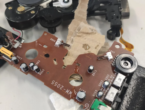
Getting PCBs made is often the key step in taking a dodgy lab experiment and turning it into a functional piece of equipment. However, it can be tedious to wait for PCBs to ship, and that can really slow down the iterative development process. If you’ve got a 3D printer, though, there’s a neat way to make your own custom PCBs. Enter PCB Forge from [castpixel].

The online tool.

The concept involves producing a base and a companion mold on your 3D printer. You then stick copper tape all over the base part, using the type that comes with conductive adhesive. This allows the construction of a fully conductive copper surface across the whole base. The companion mold is then pressed on top, pushing copper tape into all the recessed traces on the base part. You can then remove the companion mold, quickly sand off any exposed copper, and you’re left with a base with conductive traces that are ready for you to start soldering on parts. No etching, no chemicals, no routing—just 3D printed parts and a bit of copper tape. It rarely gets easier than this.

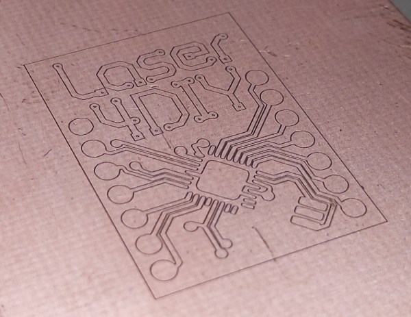
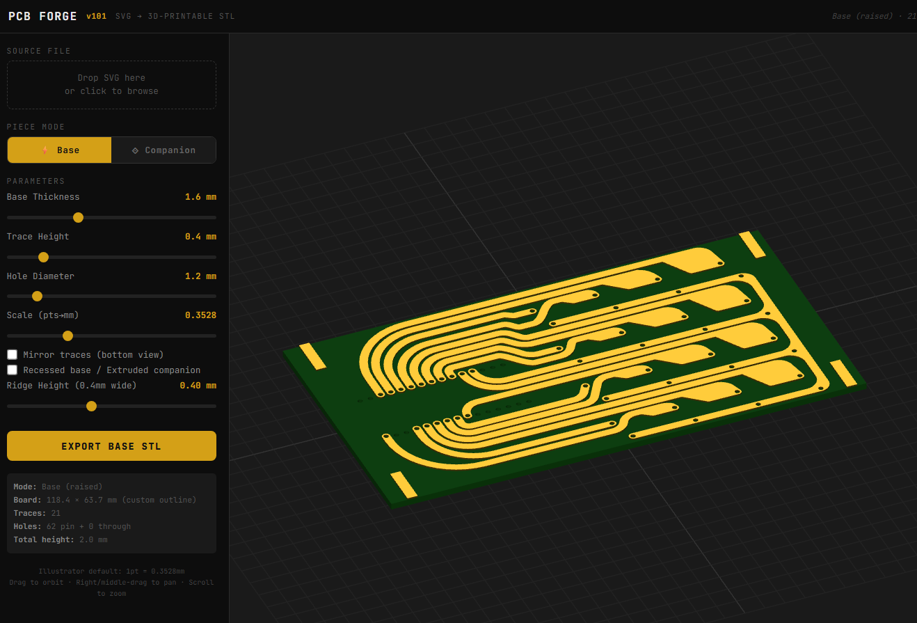
You can design your PCB traces in any vector editor, and then export a SVG. Upload that into the tool, and it will generate the 3D printable PCB for you, automatically including the right clearances and alignment features to make it a simple press-together job to pump out a basic PCB. It bears noting that you’re probably not going to produce a four-layer FPGA board doing advanced high-speed signal processing using this technique. However, for quickly prototyping something or lacing together a few modules and other components, this could really come in handy.

The work was inspired by a recent technique demonstrated by [QZW Labs], which we featured earlier this year. If you’ve got your own hacks to speed up PCB production time, or simply work around it, we’d love to know on the tipsline! Video after the break.

Continue reading “New Tool Makes 3D Printed PCBs, Fast”

A photo of the PDP-1 replica.

Hacking Printed Circuit Board To Create Casing And Instrument Panels

Over on Hackaday.io our hackers [Angelo] and [Oscarv] are making a replica of the PDP-1. That is interesting in and of itself but the particularly remarkable feature of this project is its novel use of printed circuit boards for casing and instrument panels.

What does that mean in practice? It means creating a KiCad file with a PCB for each side of the case/panel. These pieces can then be ordered from a board house and assembled. In the video below the break you will see an example of putting such a case together. They use sticky tape for scaffolding and then finish things off by soldering the solder joints on each edge together.

Continue reading “Hacking Printed Circuit Board To Create Casing And Instrument Panels”

Supercon 2024: Quick High-Feature Boards With The Circuit Graver

These days, if you want to build something with modern chips and components, you probably want a custom PCB. It lets you build a neat and compact project that has a certain level of tidiness and robustness that you can’t get with a breadboard or protoboard. The only problem is that ordering PCBs takes time, and it’s easy to grow tired of shipping delays when you don’t live in the shadow of the Shenzhen board houses.

[Zach Fredin] doesn’t suffer this problem, himself. He’s whipping up high-feature PCBs at home with speed and efficiency that any maker would envy. At the 2024 Hackaday Supercon, he was kind enough to give a talk to explain the great engineering value provided by the Circuit Graver.

Continue reading “Supercon 2024: Quick High-Feature Boards With The Circuit Graver”

Five Ways To Repair Broken PCB Traces

When everything used wires, it was easy to splice them or replace them. Not so much with PC boards, but everyone has their favorite method for repairing a broken trace. [Mr. SolderFix] has his five favorite ways, as you can see in the video below.

Of course, before you can repair a trace, you probably have to expose it since most boards have solder mask now. Unless you plan to shut the trace at both ends, exposing the actual trace is probably the first step.

Continue reading “Five Ways To Repair Broken PCB Traces”

PCB Repair Is A Sticky Proposition

What do you do when a PCB is cracked or even broken in two? [MH987] has a plan: superglue the board back and then bridge the traces with solder, solder paste, or wire. The exact method, of course, depends on the extent of the damage.

We’ve had some success with similar techniques, and, honestly, for single-sided boards, we would be tempted to add a thin backer behind the crack. We’ve also used conductive paint to repair traces, but it’s good to have having as many tricks as possible because you never know what will work best for a particular repair. The post mentions that this is easier to do on a single-sided board, but it is certainly possible to do on a two-layer board.

The example repair is a Walkman which — if you are a youngster — was a portable music player that takes cassette tapes. These haven’t been made since 2010, so it is important to repair what you have.

If you can’t repair your Walkman, you could build an updated version. If your board is seriously damaged, you might get hope from this more extreme repair.

DIY Laser For Ablating Metal

For those who wish to go beyond through-hole construction on perfboard for their circuit boards, a printed circuit board is usually the next step up. Allowing for things like surface-mount components, multi-layer boards, and a wider array of parts, they are much more versatile but do have a slight downside in that they are a little bit harder to make. There are lots of methods for producing them at home or makerspace, though, and although we’ve seen plenty of methods for their production like toner transfer, photoresist, and CNC milling, it’s also possible to make them using laser ablation, although you do need a special laser to get this job done.

The problem with cutting copper is that it reflects infra-red, so a higher-wavelength blue green laser is used instead. And because you want to ablate the copper, but not melt the surrounding areas or cut straight through the board, extremely short, high-power pulses are the way to go. Here, the [Munich Fab Lab] is using 9 kW pulses of around 30 microseconds each.  With these specifications the copper is ablated from the surface of the board allowing for fine details in the range of about 20 µm, which is fine enough for just about any circuit board. The design of the laser head itself is worth a look.

Aside from the laser, the rest is standard CNC machine fodder, but with an emphasis on safety that’s appropriate for a tool in a shared workspace, and the whole project is published under an open license and offers an affordable solution for larger-scale PCB production with extremely fine resolution and without the need for any amounts of chemicals for the more common PCB production methods. There is a lot more information available on the project’s webpage and its GitHub page as well.

Of course, there are other methods of producing PCBs by laser if you happen to have a 20 W fiber laser just kicking around.

Blinky Business Card Plays Snake And Connect Four

There’s no better way to introduce yourself than handing over a blinky PCB business card and challenging the recipient to a game of Connect Four. And if [Dennis Kaandorp] turns up early for a meeting, he can keep himself busy playing the ever popular game of Snake on his PCB business card.

The tabs are 19 mm long and 4 mm wide.

Quite wisely, [Dennis] kept his design simple, and avoided the temptation of feature creep. His requirements were to create a minimalist, credit card sized design, with his contact details printed on the silk legend, and some blinky LED’s.

The tallest component on such a design is usually the battery holder, and he could not find one that was low-profile and cheap. Drawing inspiration from The Art of Blinky Business Cards, he used the 0.8 mm thin PCB itself as the battery holder by means of flexible arms.

Connect-Four is a two player game similar to tic-tac-toe, but played on a grid seven columns across and six rows high. This meant using 42 dual-colour LED’s, which would require a large number of GPIO pins on the micro-controller. Using a clever combination of matrix and charlieplexing techniques, he was able to reduce the GPIO count down to 13 pins, while still managing to keep the track layout simple.

It also took him some extra effort to locate dual colour, red / green LED’s with a sufficiently low forward voltage drop that could work off the reduced output resulting from the use of charlieplexing. At the heart of the business card is an ATtiny1616 micro-controller that offers enough GPIO pins for the LED matrix as well as the four push button switches.

His first batch of prototypes have given him a good insight on the pricing and revealed several deficiencies that he can improve upon the next time around. [Dennis] has shared KiCad schematic and PCB layout files for anyone looking to get inspired to design their own PCB business cards.

Continue reading “Blinky Business Card Plays Snake And Connect Four”