Arduinos are a handy tool to have around. They’re versatile, cheap, easy to program, and have a ton of software libraries to build on. They’ve only been around for about a decade and a half though, so if you were living in 1989 and wanted to program a microcontroller you’d probably be stuck with an 8-bit microprocessor with no built-in peripherals to help, reading from a physical book about registers and timing, and probably trying to get a broken ribbon cable to behave so it would actually power up. If you want a less frustrating alternate history to live in, though, check out the latest project from [Marek].
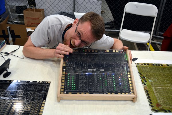
He discovered some 6502 chips (Polish language, Google Translate link) that a Chinese manufacturer was selling, but didn’t really trust that they were legitimate. On a lark he ordered some and upon testing them he found out that they were real 6502s. Building an 8-bit computer is something he’d like to do, but in the meantime he decided to do a project using one of these chips as a general-purpose microcontroller similar to a modern Arduino. The project has similar specs as an Arduino too, including 8kB of RAM memory, 8kB of I/O address space, and various EPROM capabilities. [Marek] went on to build a shield board for it as well, for easy access to some switches and LEDs. It’s a great build that anyone interested in microcontrollers should check out.
Keep in mind that an ATtiny45 has 8 bits like the 6502 but only costs around $1 USD, whereas a 6502 would have cost around $200 in today’s dollars. It’s really only in modern times that we can appreciate the 6502 as a cheap 8-bit microcontroller for that reason alone, but we can also appreciate how it ushered in a computer revolution since competing Intel and Motorola chips cost around six times more before it showed up. They became so popular in fact that people still regularly use them to build retrocomputers of all kinds.