Today, SiFive has released two new cores designed for the lower end of computing. This adds to the company’s existing portfolio of microcontrollers and SoCs based on the Open RISC-V ISA. Over the last two years, SiFive has introduced a number of cores based on the RISC-V ISA, an Open Architecture ISA that gives anyone to design and develop a microcontroller or microprocessor platform. These two new cores fill out the low-power end of SiFive’s core portfolio.
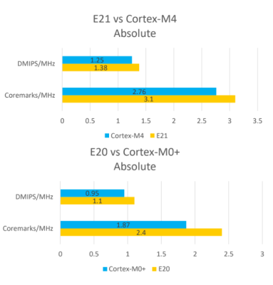
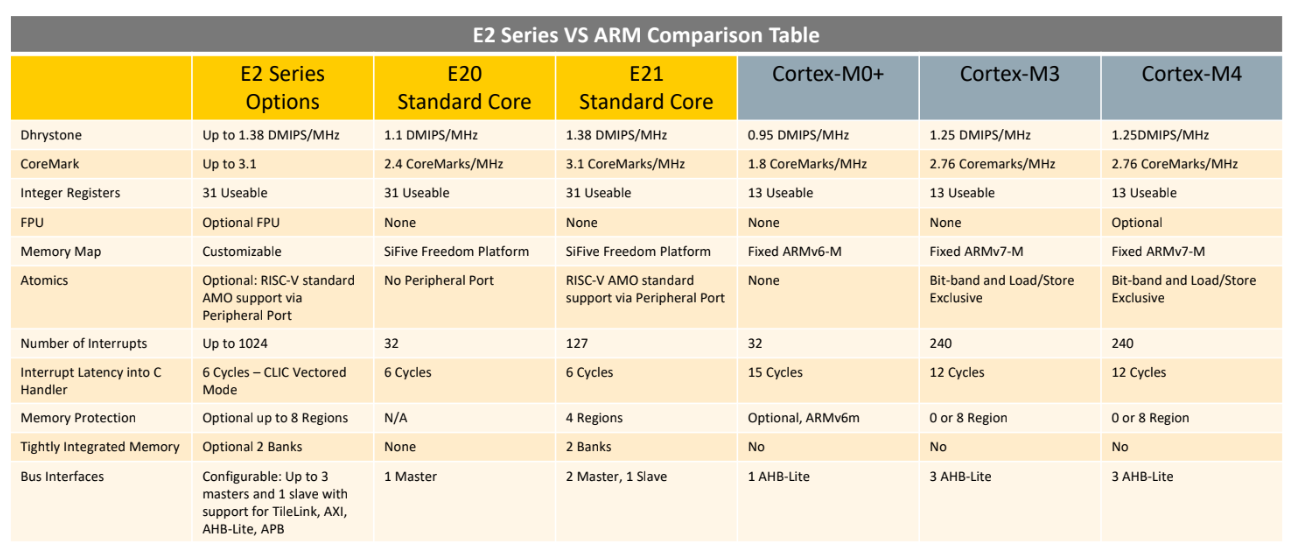
The two new cores included in the announcement are the SiFive E20 and E21, both meant for low-power applications, and according to SiFive presentations, they’re along the lines of an ARM Cortex-M0+ and ARM Cortex-M4. This is a core — it’s not a chip yet — but since the introduction of SiFive’s first microcontrollers, many companies have jumped on the RISC-V bandwagon. Western Digital, for example, has committed to using the RISC-V architecture in SoCs and as controllers for hard drive, SSDs, and NASes.
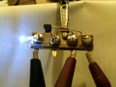
 The first chip from SiFive was the HiFive 1, which was based on the SiFive E31 CPU. We got our hands on the HiFive 1 early last year, and it is a beast. With the standard complement of benchmarks, in terms of raw power, it’s approximately twice as fast as the Teensy 3.6, based on the Kinetis K66, a 180 MHz ARM Cortex-M4F. The SiFive E31 is about 1.5 times as fast as the Teensy 3.6 on a pure calculations per clock basis. This is remarkable because the Teensy 3.6 is our go-to standard for when you want to toggle pins really really fast with a cheap, readily available microcontroller platform.
But sometimes you don’t need the fastest or best microcontroller. To that end, SiFive is looking toward a lower-power microcontroller based on the RISC-V core. The new offerings are built on the E2 Core IP series, with two standard cores. The E21 core provides mainstream performance for microcontrollers, and the E20 core is the most power-efficient core offered by SiFive. In effect, the E21 core is a replacement for the ARM Cortex-M3 and Cortex-M4, while the E20 is a replacement for the ARM Cortex-M0+.
Just a few months ago, SiFive released a gigantic, multicore, Linux-capable processor called the HiFive Unleashed. With support for DDR4 and Gigabit Ethernet, this chip would be more at home in a desktop than an Internet of Things thing. The most popular engine ever produced isn’t a seven-liter turbo diesel, it’s whatever goes into a Honda econobox; likewise, many more low-power microcontrollers like the Cortex-M0 and -M3 are sold than the newer, more powerful, and more expensive chips. Even though it’s not as exciting as a new workstation CPU, the world needs microcontrollers, and the more Open, the better.