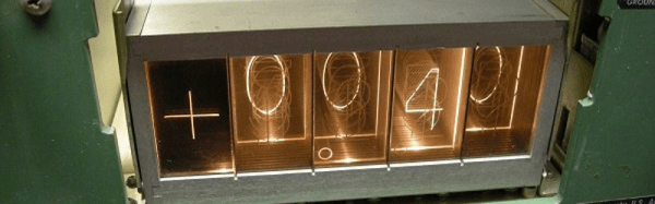
We’ve seen a bunch of replacements for nixie tubes using LEDs and edge-lit acrylic for the numbers. But one of the earliest digital voltmeters used edge-lit Lucite plates for the numbers and a lot of incandescent lamps to light them up.
[stevenjohnson] has a Non-Linear Systems Model 481 digital voltmeter and he’s done a teardown of it so we can get a glimpse of the insides. Again, anyone who’s seen the modern versions of edge-lit numeric displays knows what they are: A series of clear plastic plates with numbers (or characters) etched into them, each with a light source beneath them. You turn one light on to light one plate, another to light another, and so on. The interesting bit here is the use of incandescent bulbs and the use of sequential relays to cycle through the lights. The relays make a lot of racket, especially with the case open.
[stevenjohnson] also notes that he might have made a mistake opening up the part of the machine where the plates are stored as it took him a bit to get the plates back in place and back in the unit. We’d imagine it was pretty loud if you were taking a lot of measurements with this machine, although it looks great inside and, obviously, the idea is a pretty good one. Check out this edge-lit nixie tube display or these edge-lit numeric modules.
[via boingboing]
Continue reading “Before There Were Nixie Tubes, There Were Edge-Lit Displays?”
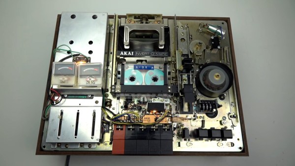
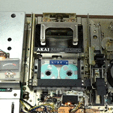 Towards the end of the cassette era, most manufacturers had decided on a relatively simple system of having the head assembly rotate while reversing the motor direction. Many years prior to this, however, Akai’s system involved a shuttle which carried the tape up to a rotating arm that flipped the cassette, before shuttling it back down and reinserting it into the deck.