We’ve become sadly accustomed to consumer devices that seem to give up the ghost right after the warranty period expires. And even when we get “lucky” and the device fails while it’s still covered, chances are that there will be no attempt to repair it; the unit will be replaced with a new one, and the failed one will get pitched in the e-waste bin.
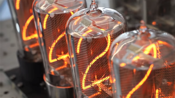
Not every manufacturer takes this approach, however. When premium quality is the keystone of your brand, you need to take field failures seriously. [Dalibor Farný], maker of high-end Nixie tubes and the sleek, sophisticated clocks they plug into, realizes this, and a new video goes into depth about the process he uses to diagnose issues and prevent them in the future.
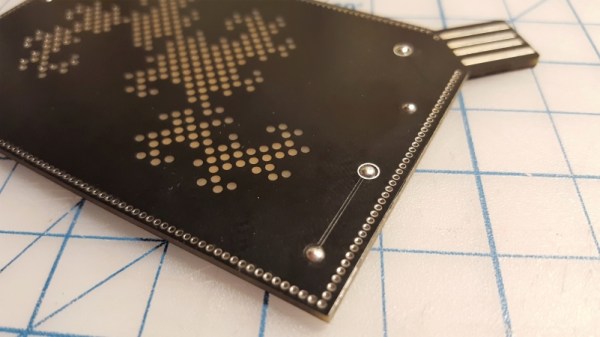
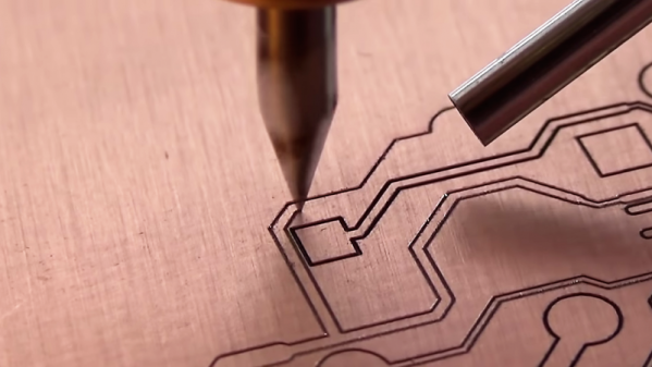
One clock with a digit stuck off was traced to via failure by barrel fatigue, or the board material cracking inside the via hole and breaking the plated-through copper. This prompted a board redesign to increase the diameter of all the vias, eliminating that failure mode. Another clock had a digit stuck on, which ended up being a short to ground caused by pin misalignment; when the tube was plugged in, the pins slipped and scraped some solder off the socket and onto the ground plane of the board. That resulted in another redesign that not only fixed the problem by eliminating the ground plane on the upper side of the board, but also improved the aesthetics of the board dramatically.
As with all things [Dalibor], the video is a feast for the eyes with the warm orange glow in the polished glass and chrome tubes contrasting with the bead-blasted aluminum chassis. If you haven’t watched the “making of” video yet, you’ve got to check that out too.
Continue reading “Nixie Clock Failure Analysis, [Dalibor Farný] Style”