How Does The Raspberry Pi Rack Up Against A Mini PC?

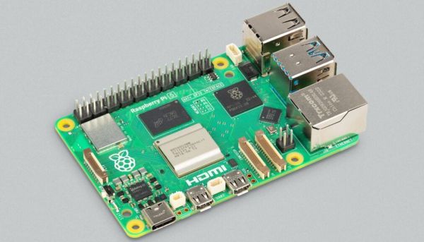
When the first Raspberry Pi came out back in 2012 it was groundbreaking because it offered a usable little Linux machine with the proud boast of a $25 dollar price tag. Sure it wasn’t the fastest kid on the block, but there was almost nothing at that price which could do what it did. Three leap years later though it’s surrounded by a host of competitors with similar hardware, and its top-end model now costs several times that original list price.

Meanwhile the cost of a “real” x86 computer such as those based upon the Intel N100 has dropped to the point at which it almost matches a fully tricked-out Pi with storage and peripherals, so does the Pi still hold its own? [CNX Software] has taken a look.

From the examples they use, in both cases the Intel machine is a little more expensive than the Pi, but comes with the advantage of all the peripherals, cooling, and storage coming built-in rather than add-ons. They rate the Pi as having the advantage on expandability as we’d expect, but the Intel giving a better bang for the buck in performance terms. From where we’re sitting the advantage of the Pi over most of its ARM competition has always been its good OS support, something which is probably exceeded by that on an x86 platform.

So, would you buy the Intel over the high-end Pi? Let us know in the comments.

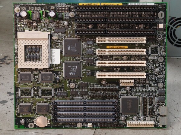
PC AT mainboard with both 16-bit ISA and 32-bit PCI slots. (Credit: htomari, Flickr)

How Intel Gave Us The PCI Bus While Burying VESA’s VL-Bus

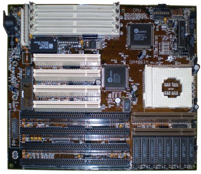
Gigabyte GA486IM mainboard from 1994 with ISA, VLB and PCI slots. (Credit: Rjluna2, Wikimedia)

The early days of home computing were quite a jungle of different standards and convoluted solutions to make one piece of hardware work on as many different platforms as possible. IBM’s PC was an unexpected shift here, as with its expansion card-based system (retroactively called the ISA bus) it inspired a new evolution in computers. Of course, by the early 1990s the ISA bus couldn’t keep up with hardware demands, and a successor was needed. Many expected this to be VESA’s VLB, but as [Ernie Smith] regales us in a recent article in Tedium, Intel came out of left field with its PCI standard after initially backing VLB.

IBM, of course, wanted to see its own proprietary MCA standard used, while VLB was an open standard. One big issue with VLB is that it isn’t a new bus as such, but rather an additional slot tacked onto the existing ISA bus, as it was then called. While the reasoning for PCI was sound, with it being a compact, 32-bit (also 64-bit) design with plug and play and more complex but also more powerful PCI controller, its announcement came right before VLB was supposed to be announced.

Although there was some worry that having both VLB and PCI in the market competing would be bad, ultimately few mainboards ended up supporting VLB, and VLB quietly vanished. Later on PCI was extended into the Accelerated Graphics Port (AGP) that enabled the GPU revolution of the late 90s and still coexists with its PCIe successor. We covered making your own ISA and PCI cards a while ago, which shows that although PCI is more complex than ISA, it’s still well within the reach of today’s hobbyist, unlike PCIe which ramps up the hardware requirements.

Top image: PC AT mainboard with both 16-bit ISA and 32-bit PCI slots. (Credit: htomari, Flickr)

Two pictures of the mobo side by side, both with kapton tape covering everything other than the flash chip. On the left, the flash chip is populated, whereas on the right it's not

Enabling Intel AMT For BIOS-over-WiFi

Intel ME, AMT, SMT, V-Pro… All of these acronyms are kind of intimidating, all we know about them is that they are tied to remote control technologies rooted deep in Intel CPUs, way deeper than even operating systems go. Sometimes though, you want remote control for your own purposes, and that’s what [ABy] achieved. He’s got a HP ProDesk 600 G3 Mini, decided to put it into a hard to reach spot in his flat, somewhere you couldn’t easily fetch a monitor and a keyboard for any debugging needs. So, he started looking into some sort of remote access option in case he’d need to access the BIOS remotely, and went as far as it took to make it work. (Google Translate)

The features he needed are covered by Intel AMT — specifically, BIOS access over a WiFi connection. However, his mini PC only had SMT enabled from the factory, the cut-down version of AMT without features like wireless support. He figured out that BIOS dumping was the way, promptly did just that, found a suitable set of tools for his ME region version, and enabled AMT using Intel’s FIT (Flash Image Tool) software.

Now, dumping the image could be done from a running system fully through software, but apparently, flashing back requires an external programmer. He went with the classic CH341, did the 3.3 V voltmod that’s required to make it safe for flash chip use, and proceeded to spend a good amount of time making it work. Something about the process was screwy, likely the proprietary CH341 software. Comments under the article highlight that you should use flashrom for these tasks, and indeed, you should.

This article goes into a ton of detail when it comes to working with Intel BIOS images — whichever kind of setting you want to change, be it AMT support or some entirely different but just as tasty setting, you will be well served by this write-up. Comments do point out that you might want to upgrade the Intel ME version while at it, and for what it’s worth, you can look into disabling it too; we’ve shown you a multitude of reasons why you should, and a good few ways you could.

50-Year-Old Program Gets Speed Boost

At first glance, getting a computer program to run faster than the first electronic computers might seem trivial. After all, most of us carry enormously powerful processors in our pockets every day as if that’s normal. But [Mark] isn’t trying to beat computers like the ENIAC with a mobile ARM processor or other modern device. He’s now programming with the successor to the original Intel integrated circuit processor, the 4040, but beating the ENIAC is still little more complicated than you might think with a processor from 1974.

For this project, the goal was to best the 70-hour time set by ENIAC for computing the first 2035 digits of pi. There are a number of algorithms for performing this calculation, but using a 4-bit processor and an extremely limited memory of only 1280 bytes makes a number of these methods impossible, especially with the self-imposed time limit. The limited instruction set is a potential bottleneck as well with these early processors. [Mark] decided to use [Fabrice Bellard]’s algorithm given these limitations. He goes into great detail about the mathematics behind this method before coding it in JavaScript. Generating assembly language from a working JavaScript was found to be fairly straightforward.

[Mark] is also doing a lot of work on the 4040 to get this program running as well, including upgrades to the 40xx tool stack, the compiler and linker, and an emulator he’s using to test his program before sending it to physical hardware. The project is remarkably well-documented, including all of the optimizations needed to get these antique processors running fast enough to beat the ENIAC. We won’t spoil the results for you, but as a hint to how it worked out, he started this project using the 4040 since his original attempt using a 4004 wasn’t quite fast enough.

Finally, An Open-Source 8088 BIOS

The Intel 8088 is an interesting chip, being a variant of the more well-known 8086. Given the latter went on to lend its designation to one of the world’s favorite architectures, you can tell which of the two was higher status. Regardless, it was the 8088 that lived in the first IBM PC, and now, it even has its own open-source BIOS.

As with any BIOS, or Basic Input Output System, it’s charged with handling core low-level features for computers like the Micro 8088, Xi 8088, and NuXT. It handles chipset identification, keyboard and mouse communication, real-time clock, and display initialization, among other things.

Of course, BIOSes for 8088-based machines already exist. However, in many cases, they are considered to be proprietary code that cannot be freely shared over the internet. For retrocomputing enthusiasts, it’s of great value to have a open-source BIOS that can be shared, modified, and tweaked as needed to suit a wide variety of end uses.

If you want to learn more about the 8088 CPU, we’ve looked in depth at that topic before. Feel free to drop us a line with your own retro Intel hacks if you’ve got them kicking around!

[Ken] Looks At The 386

The 80386 was — arguably — Intel’s first modern CPU. The 8086 was commercially successful, but the paged memory model was stifling. The 80286 also had a protected mode, which differed from the 386’s. [Ken Shirriff] takes the 386 apart for us in a recent blog post.

The 286’s protected mode was less successful than the 386 because of several key limitations as it was a 16-bit processor with a 24-bit address bus. It still required segment changes to access larger amounts of memory, and it had no good way to call back into real mode for compatibility reasons. The 386 fixed all that. You could adopt a segment strategy if you wanted to. But you could also load the segment registers once to point to a 4 GB linear address space and then essentially forget them. You also had a virtual 86 mode that could simulate real mode with some work.

The CPU used a 1-micron process, compared to the 1.5-micron process used earlier. The chip had 285,000 transistors (although the 80386SL had many more). That was ten times the number of devices on the 8086. The cheaper 386SX did use the 1.5 micron process for a while, but with a 16-bit external bus, this was feasible. While 285,000 sounds like a lot, a Core i9 has around 4.2 billion transistors. Times have changed.

A smaller design also allowed chips like the 386SL for laptops. The CPU took up only about a fourth of the die. The rest held bus controllers and cache interfaces to cut costs on laptops. That’s why it had so many more transistors.

[Ken] does his usual in-depth analysis of both the die and the history behind this historic device. We spent a lot of time writing protected mode 386 code, and it was nice to see the details of a very old friend. These days, you can get a pretty capable CPU system on a solderless breadboard, but designing a working 386 system took a few extra parts. The 80286 was a stepping stone between the 8086 and 80386, but even it had some secrets to give up.

Intel’s Chips Light The Way To Faster Processor Arrays

It’s very likely indeed that whatever you are reading this on will have a multi-core processor. They’re now the norm, but the path to they octa-or-more-core chip in your phone has gone from individual processors with PCB interconnects through many generations of ever faster on-chip ones.

But what if your power needs are so high-end that you need more cores that can be fitted on one chip, but without the slow PCB interconnect to another? If you’re Intel, you develop a multi-core processor with an on-chip photonic interconnect. It talks to the neighboring ones in its cluster at full speed, via light.

The chip in question isn’t one you’ll see in a machine near you, instead it’s inspired by the extremely demanding requirements for DARPA’s HIVE graph analytics program. So this is a machine for supercomputers in huge data centers rather than desktop computers, it will be assembled into multi-die packages with that chip-to-chip optical networking built in. But your computer today is the equal of a supercomputer from not that many years ago, so never say you won’t one day be using its descendant technologies.