Hybrid 3D-Printer Creates Complete Circuits, Case And All

The cool kids these days all seem to think we’re on the verge of an AI apocalypse, at least judging by all the virtual ink expended on various theories. But our putative AI overlords will have a hard time taking over the world without being able to build robotic legions to impose their will. That’s why this advance in 3D printing that can incorporate electronic circuits may be a little terrifying, at least to some.

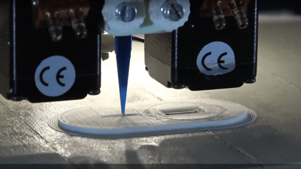
The basic idea that [Florens Wasserfall] and colleagues at the University of Hamburg have come up with is a 3D-printer with a few special modifications. One is a separate extruder than squirts a conductive silver-polymer ink, the other is a simple vacuum tip on the printer extruder for pick and place operations. The bed of the printer also has a tray for storing SMD parts and cameras for the pick-and-place to locate parts and orient them before placing them into the uncured conductive ink traces.

The key to making the hardware work together though is a toolchain that allows circuits to be integrated into the print. It starts with a schematic in Eagle, which joins with the CAD model of the part to be printed in a modified version of Slic3r, the open-source slicing package. Locations for SMD components are defined, traces are routed, and the hybrid printer builds the whole assembly at once. The video below shows it in action, and we’ve got to say it’s pretty slick.

Sure, it’s all academic for now, with simple blinky light circuits and the like. But team this up with something like these PCB motors, and you’ve got the makings of a robotic nightmare. Or not.

Continue reading “Hybrid 3D-Printer Creates Complete Circuits, Case And All”

Play With A Papercraft Electronics Activity Book

As conductive ink becomes readily available and in greater varieties, we’re starting to see some intriguing applications. [Marion Pinaffo] and [Raphaël Pluviange] created a book of papercraft projects that employ silver-based ink for making a circuit’s wires, carbon-based ink for resistance, as well as color-changing ink. Electronics components’ leads are slipped into slits cut into the paper, connected to conductive-ink traces.

[Marion] and [Raphaël] use 555s, ATtiny85s, watch batteries, and other hardware to make each activity or project unique. A number of projects use a rolling ball bearing to make beeps in a piezo speaker. They also created beautifully designed pages to go with the electronics.

It looks like a fun way for neophytes to play around with electronics, and once the paper part is kaput, the user would be left with the hardware. Imagine one of those beginners googling to find the pinout of the Tiny85 or discovering the Stepped Tone Generator and makes one with the 555.

If you like this project you’ll appreciate the working papercraft organ and papercraft resistor calculator we previously published.

Continue reading “Play With A Papercraft Electronics Activity Book”

Can You Build An E-ink Display From Scratch?

Modern displays are fascinating little things. In particular, the E-Ink displays employed in modern E-books achieve mesmerising paper like contrast with excellent standby power consumption.  Many of us at some point have had a go at experimenting with DIY displays, but been discouraged by the miniature scales involved. Driving them is hard enough, but building your own?

[MChel] has achieved some excellent success in building a simple E-Ink display. The account presented on this Russian electronics forum, graciously translated for us by Google Translate, outlines that the greatest barrier to pursing this in your home lab is creating the conductive layer that serve as electrodes for each pixel and depositing the thin layer of electrostatically charged ink pellets onto another transparent yet conductive film. [MChel] solution was to extract a small a portion of pre-deposited ink from a smashed and notoriously brittle E-ink display. Next, instead of attempting to build an ambitious and dense grid of electrodes, [MChel] etched a simple battery indicator on a PCB. The ink and the electrodes were then fused with some DIY graphite based conductive glue and sealed with some careful yet ingenuitive epoxy laying skills.

The DIY electrodes

The result is a working battery indicator that consumes no power, whilst reporting any remaining power.

There is something increasingly defiant and laudable about home-brewing technologies, otherwise thought to be confined to multi-million dollar factories. We have already covered how you should go about making some conductive glass and using it in your homemade LCD.

Retrotechtacular: Whatever Happened To The Paper Mobile Phone

It was one of the more interesting consumer tech stories floating around at the turn of the century, a disposable cell phone manufactured using a multi-layer folded paper circuit board with tracks printed in conductive ink. Its feature set was basic even by the standards of the day in that it had no display and its only function was to make calls, but with a target price of only $10 that didn’t matter. It was the brainchild of a prolific New Jersey based inventor, and it was intended to be the first in a series of paper electronic devices using the same technology including phones with built-in credit card payment ability and a basic laptop model.

The idea of a $10 mobile phone does not seem remarkable today, it’s possible that sum might now secure you something with features far in excess of the Nokias and similar that were the order of the day at that time. But when you consider that those Nokias could have prices well into three figures without a contract, and that the new features people considered exciting were things like integrated antennas or swappable coloured plastic covers rather than the multicore processors or high-res cameras we’re used to today, a phone so cheap as to be disposable promised to be very disruptive.

The web site publicity shot for the disposable paper phone.

The product’s wonderfully dated website (Wayback Machine link, we’ve skipped the Flash intro for you) has pictures of the device, and the video below the break features shots of it in use as its inventor is interviewed. But by the end of 2002 the Wayback Machine was retrieving 404 errors from the server, and little more was heard of the product. No sign of one ever came our way; did any make it to market, and did you have one?

With the benefit of fifteen years hindsight, why did we not have paper mobile phones as part of the ephemera of the early years of the last decade? It was not a product without promise; a ten-dollar phone might have been a great success. And the description of a cheap laptop that talks to a remote server for its software sounds not unlike today’s Chromebooks.

Some of you might claim the product was vapourware, but given that they demonstrated a working prototype we’d hesitate to go that far. The likelihood is that it did not find the required combination of component price and manufacturing ease to exploit its intended market segment before its competition improved to the point that it could no longer compete. If you have ever taken apart a typical mobile phone of the period you’ll have some idea of why they were not cheap devices, for example the RF filter modules of the day were individually adjusted precision components. And paper-and-ink printed circuit boards are still a technology with a way to go even now, perhaps the idea was simply too far ahead of its time. Meanwhile within a relatively short period of time the price of simple candybar phones dropped to the point at which they would tempt the $10 buyer to spend more for a better product, so the window of opportunity had passed.

Continue reading “Retrotechtacular: Whatever Happened To The Paper Mobile Phone”

Conductive Circuit Board Tattoos: Tech Tats

While hardcore body-hackers are starting to freak us out with embedded circuit boards under their skin, a new more realistic option is becoming available — temporary tech tattoos. They’re basically wearable circuit boards.

Produced by [Chaotic Moon], the team is excited to explore the future of skin-mounted components — connected with conductive ink in the form of a temporary tattoo. And if you’re still thinking why, consider this. If these tattoos can be used as temporary health sensors, packed with different biometric readings, the “tech tat” can be applied when it is needed, in order to monitor specific things.

In one of their test cases, they mount an ATiny85 connected to temperature sensors and an ambient light sensor on the skin. A simple device like this could be used to monitor someone’s vitals after surgery, or could even be used as a fitness tracker. Add a BLE chip, and you’ve got wireless data transfer to your phone or tablet for further data processing.

Continue reading “Conductive Circuit Board Tattoos: Tech Tats”

Easier PCB Vias With Drill Trick And Conductive Ink

If you’ve ever made double-sided PCBs without professional equipment, you had to deal with connecting one side of the board to the other. You have a few obvious choices: 1) Rely on component leads to connect both sides (and solder both sides); 2) Create vias and solder wire to both sides of the board; or 3) Use through hole rivets. [Diyouware] had a different idea: use conductive ink. After a few false starts, they found a technique that seemed to work well.

This isn’t the first time we’ve heard of people trying conductive ink with varying degrees of success. The biggest problem, usually, is that the ink wants to run out of the hole. [Diyouware] has an interesting solution for this problem: Don’t drill the hole all the way thorough.

Continue reading “Easier PCB Vias With Drill Trick And Conductive Ink”

Ask Hackaday: Are Conductive Inks Going To Make It?

It’s amazing how affordable PCB fabrication has become. It has long been economical (although not always simple) to fabricate your own singe and double-sided boards at home, the access to professional fabrication is becoming universal. The drive continues downward for both cost and turnaround time. But there is growing interest in the non-traditional.

Over the last year we’ve seen a huge push for conductive-ink-based PCB techniques. These target small-run prototyping and utilize metals (usually silver) suspended in fluid (think glue) to draw traces rather than etching the traces out of a single thin layer of copper. Our question: do you think conductive in will become a viable prototyping option?

Voltera V-One Circuit Board Prototyping Machine

I recorded this interview at 2015 CES but was asked not to publish it until their crowd funding campaign went live. If you haven’t been paying attention, Voltera is at almost 400% of their $70k goal with 26 days remaining. This printer definitely works. You can print circuits, solder components or reflow them, and there’s even a second non-conductive ink that can be used to insulate between traces when they cross over one another. In the video [Alroy] suggests Voltera for small production runs of 10-20 boards. Would you see yourself using this for 10-20 boards?

Personally, I think I could solder point-to-point prototypes in less time. Consider this: the V-One will print your traces but you still must solder on the components yourself. If the board design reaches a high level of complexity, that timing may change, but how does the increased resistance of the ink compared to copper traces affect the viability of a board? I assume that something too complex to solder point-to-point would be delving into high-frequency communications (think parallel bus for LCD displays, etc.). Is my assumption correct? Do you think conductive ink will get to the point that this is both viable and desirable over etching your own prototypes and how long before we get there?

Now, I certainly do see some perfect use-cases for Voltera. For instance, introduction to circuit design classes. If you had one of these printers at the middle school or high school level it would jump-start interest in electronics engineering. Without the need for keeping chemical baths like Cuperic Chloride or Ferric Chloride on hand, you could walk students through simple board design and population, with the final product to take home with them. That’s a vision I can definitely get behind and one that I think will unlock the next generation of hardware hackers.

Correction: [Arachnidster] pointed out in the comments that Voltera is still working on being able to reflow boards printed by the V-One. On their Kickstarter page they mention: “(Reflow onto Voltera printed boards is currently under development)”