The Perils Of Return Path Gaps

The radio frequency world is full of mysteries, some of which seem to take a lifetime to master. And even then, it seems like there’s always something more to learn, and some new subtlety that can turn a good design on paper into a nightmare of unwanted interference and unexpected consequences in the real world.

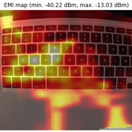
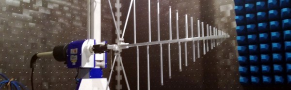
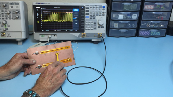
As [Ken Wyatt] aptly demonstrates in the video below, where you put gaps in return paths on a PCB is one way to really screw things up. His demo system is simple: a pair of insulated wires running from the center pins on BNC jacks and running along the surface of a piece of copper-clad board to simulate a PCB trace. The end of each wire is connected to the board’s ground plane through a 50 ohm resistor, with one wire running over a narrow slot cut into the board. A harmonics-rich signal is fed into each trace while an H-field EMC probe connected to a spectrum analyzer is run along the length of the trace.

With the trace running over the solid ground plane, the harmonics are plentiful, as expected, but they fall off very quickly away from the trace. But over on the trace with the gapped return trace it’s a far different story. The harmonics are still there, but they’re about 5 dBmV higher in the vicinity of the gap. [Ken] also uses the probe to show just how far from the signal trace the return path extends to get around the gap. And even worse, the gap makes it so that harmonics are detectable on the unpowered trace. He also uses a current probe to show how common-mode current will radiate from a long conductor attached to the backplane, and that it’s about 20 dB higher with the gapped trace.

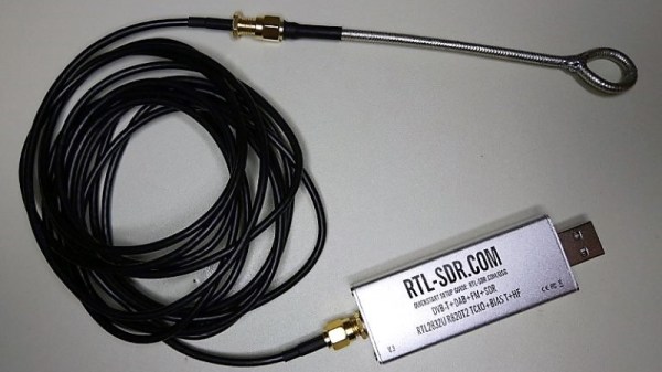
Hats off to [Ken] for this simple explanation and vivid reminder to watch return paths on clock traces and other high-frequency signals. Need an EMC probe to check your work? A bit of rigid coax and an SDR are all you needContinue reading “The Perils Of Return Path Gaps”

Homebrew TEM Cell Lets You EMC Test Your Own Devices

Submitting a new device for electromagnetic compatibility (EMC) testing seems a little like showing up for the final exam after skipping all the lectures. You might get lucky and pass, but it really would have been smarter to take a few of the quizzes to see how things were going during the semester. Similarly, it would be nice to know you’re not making any boneheaded mistakes early in the design process, which is what this DIY TEM cell is all about.

We really like [Petteri Aimonen]’s explanation of what a TEM cell, or transverse electromagnetic cell, is: he describes it as “an expanded coaxial cable that is wide enough to put your device inside of.” It basically a cage made of conductive material that encloses a space for the device under test, along with a stripline going down its center. The outer cage is attached to the outer braid of a coaxial cable, while the stripline is connected to the center conductor. Any electric or magnetic field generated by the device inside the cage goes down the coax into your test instrument, typically a spectrum analyzer.

[Petteri]’s homebrew TEM is made from a common enough material: copper-clad FR4. You could use double-sided material, or even sheet copper if you’re rich, but PCB stock is easy to work with and gets the job done. His design is detailed in a second post, which goes through the process of designing the size and shapes of all the parts as well as CNC milling the sheets of material. [Petteri] tried to make the joints by milling part-way through the substrate and bending the sheet into shape, but sadly, the copper didn’t want to cooperate with his PCB origami. Luckily, copper foil tape and a little solder heal all wounds. He also incorporated a line impedance stabilization network (LISN) into the build to provide a consistent 50-ohm characteristic impedance.

How does it work? Pretty well, it seems; when connected to a TinySA spectrum analyzer, [Petteri] was able to find high-frequency conductive noise coming from the flyback section of a switch-mode power supply. All it took was a ferrite bead and cap to fix it early in the prototyping phase of the project. Sounds like a win to us.

Make Some Noise Or Simulate It, At Least

Noise is a fact of life, especially in electronic circuits. But on our paper schematics and just as often our simulations, there is no noise. If you are blinking an LED on a breadboard, you probably don’t care. But if you are working on something meatier, handling electrical noise gracefully is important and simulation can help you. [Ignacio de Mendizábal] has a great piece on simulating EMC filters using LTSpice that can get you started.

There are many ways of classifying noise and [Ignacio] starts with common-mode versus differential noise, where common-mode is noise with current flowing in the same direction without regard to the circuit’s normal operation, and differential noise having currents that flow in the opposite direction of normal current flow.

Continue reading “Make Some Noise Or Simulate It, At Least”

Camera Sees Electromagnetic Interference Using An SDR And Machine Vision

It’s one thing to know that your device is leaking electromagnetic interference (EMI), but if you really want to solve the problem, it might be helpful to know where the emissions are coming from. This heat-mapping EMI probe will answer that question, with style. It uses a webcam to record an EMI probe and the overlay a heat map of the interference on the image itself.

Regular readers will note that the hardware end of [Charles Grassin]’s EMI mapper bears a strong resemblance to the EMC probe made from semi-rigid coax we featured recently. Built as a cheap DIY substitute for an expensive off-the-shelf probe set for electromagnetic testing, the probe was super simple: just a semi-rigid coax jumper with one SMA plug lopped off and the raw end looped back and soldered. Connected to an SDR dongle, the probe proved useful for tracking down noisy circuits.

[Charles]’ project takes that a step further by adding a camera that looks down upon the device under test. OpenCV is used to track the probe, which is moved over the DUT manually with the help of an augmented reality display that helps track coverage, with a Python script recording its position and the RF power measurements. The video below shows the capture process and what the data looks like when reassembled as an overlay on top of the device.

Even if EMC testing isn’t your thing, this one seems like a lot of fun for the curious. [Charles] has kindly made the sources available on GitHub, so this is a great project to just knock out quickly and start mapping.

Continue reading “Camera Sees Electromagnetic Interference Using An SDR And Machine Vision”

A DIY EMC Probe From Semi-Rigid Coax And An SDR

Do you have an EMC probe in your toolkit? Probably not, unless you’re in the business of electromagnetic compatibility testing or getting a product ready for the regulatory compliance process. Usually such probes are used in anechoic chambers and connected to sophisticated gear like spectrum analyzers – expensive stuff. But there are ways to probe the electromagnetic mysteries of your projects on the cheap, as this DIY EMC testing setup proves.

As with many projects, [dimtass]’ build was inspired by a video over on EEVblog, where [Dave] made a simple EMC probe from a length of semi-rigid coax cable. At $10, it’s a cheap solution, but lacking a spectrum analyzer like the one that [Dave] plugged his cheap probe into, [dimtass] went a different way. With the homemade probe plugged into an RTL-SDR dongle and SDR# running on a PC, [dimtass] was able to get a decent approximation of a spectrum analyzer, at least when tested against a 10-MHz oven-controlled crystal oscillator. It’s not the same thing as a dedicated spectrum analyzer – limited bandwidth, higher noise, and not calibrated – but it works well enough, and as [dimtass] points out, infinitely hackable through the SDR# API. The probe even works decently when plugged right into a DSO with the FFT function running.

Again, neither of these setups is a substitute for proper EMC testing, but it’ll probably do for the home gamer. If you want to check out the lengths the pros go through to make sure their products don’t spew signals, check out [Jenny]’s overview of the EMC testing process.

[via RTL-SDR.com]

One Man’s Tale Of EMC Compliance Testing

If you turn over almost any electronic device, you should find all those compliance logos: CE, FCC, UL, TÜV, and friends. They mean that the device meets required standards set by a particular region or testing organisation, and is safe for you, the consumer.

Among those standards are those concerning EMC, or ElectroMagnetic Compatibility. These ensure that the device neither emits RF radiation such that it might interfere with anything in its surroundings, nor is it unusually susceptible to radiation from those surroundings. Achieving a pass in those tests is something of a black art, and it’s one that [Pero] has detailed his exposure to in the process of seeing a large 3-phase power supply through them. It’s a lengthy, and fascinating post.

He takes us through a basic though slightly redacted look at the device itself, before describing the testing process, and the EMC lab. These are fascinating places with expert staff who can really help, though they are extremely expensive to book time in. Since the test involves a mains power supply he describes the Line Impedance Stabilisation Network, or LISN, whose job is to safely filter away the RF component on the mains cable, and present a uniform impedance to the device.

In the end his device failed its test, and he was only able to achieve a pass with a bit of that black magic involving the RF compliance engineer’s secret weapons: copper tape and ferrite rings. [Pero] and his colleagues are going to have to redesign their shielding.

We’ve covered our visits to the EMC test lab here before.

An Overview Of The Dreaded EMC Tests

There is one man whose hour-long sessions in my company give me days of stress and worry. He can be found in a soundless and windowless room deep in the bowels of an anonymous building in a town on the outskirts of London. You’ve probably driven past it or others like it worldwide, without being aware of the sinister instruments  that lie within.

The man in question is sometimes there to please the demands of the State, but there’s nothing too scary about him. Instead he’s an engineer and expert in electromagnetic compatibility, and the windowless room is a metal-walled and RF-proof EMC lab lined with ferrite tiles and conductive foam spikes. I’m there with the friend on whose work I lend a hand from time to time, and we’re about to discover whether all our efforts have been in vain as the piece of equipment over which we’ve toiled faces a battery of RF-related tests. As before when I’ve described working on products of this nature the specifics are subject to NDAs and in this case there is a strict no-cameras policy at the EMC lab, so yet again my apologies as any pictures and specifics will be generic.

There are two broadly different sets of tests which our equipment will face: RF radiation, and RF injection. In simple terms: what RF does it emit, and what happens when you push RF into it through its connectors and cables? We’ll look at each in turn as a broad overview pitched at those who’ve never seen inside an EMC lab, sadly there simply isn’t enough space in a Hackaday article to cover every nuance.

Continue reading “An Overview Of The Dreaded EMC Tests”