Additive Manufacturing Of Nickel Nanopillars Using Two-Photon Lithography

The multistep, two-photon-lithography-based additive manufacturing method forms intermediate products of blank polymer, Ni-infused polymer, and NiO while fabricating Ni
nanopillars. (Credit: Zhang et al., 2023)

Manufacturing nano-sized features is rapidly becoming an essential part of new technologies and process, ranging from catalysts to photonics and nano-scale robotics. Creating these features at scale and in a reproducible manner is a challenge, with previous attempts using methods ranging from dealloying and focused ion beams to templated electrodeposition all coming with their own drawbacks. Here recent research by Whenxin Zhang and colleagues as published in Nano Letters demonstrates a method using additive manufacturing.

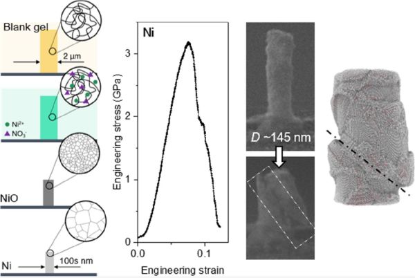
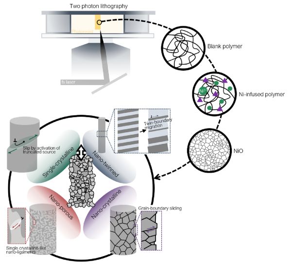
Specifically, nanopillars were printed in a hydrogel polymer with a laser-based lithography method called two-photon absorption which allows for a femtosecond laser to very precisely affect a small region within the targeted material with little impact on the surrounding area. This now solid and structured polymer hydrogel was then submerged into a Ni(NO3)2 solution to infuse it with nickel. After drying, the resulting structure had the polymer burned away in a furnace, leaving just the porous Ni nanopillars.

Subsequent testing showed that these nanopillars were more robust than similar structures created using other methods, presumably due to the less ordered internal physical structure of each pillar. Based on these results, it’s likely that the same approach could be used for other types of nano-sized structures.

A wafer being loaded into an electron microscope

Using Electron Beams To Draw Tiny Shapes Onto Silicon

Over the past few years we’ve seen several impressive projects where people try to manufacture integrated circuits using hobbyist tools. One of the most complex parts of this process is lithography: the step in which shapes are drawn onto a silicon wafer. There are several ways to do this, all of them rather complicated, but [Zachary Tong] over at Breaking Taps has managed to make one of them work quite well. He shares the results of his electron-beam lithography experiments in his latest video (embedded below).

In e-beam lithography, or EBL, shapes are drawn onto a wafer using an electron beam in a vacuum chamber. This is a slow process compared to optical lithography, as used in mass production, but it is reasonably simple and very flexible. [Zach] decided to use his electron microscope as an e-beam litho machine; although not designed for lithography, it has the same basic components as a real EBL machine and can act as a substitute with a bit of software tweaking.

An AFM image of Rick Astley
[Zach] also has an atomic force microscope, which he used to make these beautiful images.
The first step is to coat a wafer with a layer of e-beam resist. [Zach] used PMMA, commonly known as acrylic plastic, and applied it using spin coating after dissolving it in anisole. He then placed the wafer into the electron microscope and used it to scan an image. The image was then developed by rinsing the wafer in cold isopropyl alcohol.

[Zach] explains the whole process in detail in his video, including how he tuned all the parameters like resist thickness, beam strength, exposure time and development time, as well as the software tricks needed to persuade the microscope to function as a litho machine. In his best runs he managed to draw lines with a width of about 100 nanometers, which is seriously impressive for such a relatively simple setup.

These e-beam lithography experiments follow on from [Zach]’s earlier research using lasers. Homebrew IC expert Sam Zeloof has also used electron beams in his work. Thanks for the tip, [smellsofbikes]!

Continue reading “Using Electron Beams To Draw Tiny Shapes Onto Silicon”

Old Printer Becomes Direct Laser Lithography Machine

What does it take to make your own integrated circuits at home? It’s a question that relatively few intrepid hackers have tried to answer, and the answer is usually something along the lines of “a lot of second-hand equipment.” But it doesn’t all have to be cast-offs from a semiconductor fab, as [Zachary Tong] shows us with his homebrew direct laser lithography setup.

Most of us are familiar with masked photolithography thanks to the age-old process of making PCBs using photoresist — a copper-clad board is treated with a photopolymer, a mask containing the traces to be etched is applied, and the board is exposed to UV light, which selectively hardens the resist layer before etching. [Zach] explores a variation on that theme — maskless photolithography — as well as scaling it down considerably with this rig. An optical bench focuses and directs a UV laser into a galvanometer that was salvaged from an old laser printer. The galvo controls the position of the collimated laser beam very precisely before focusing it on a microscope that greatly narrows its field. The laser dances over the surface of a silicon wafer covered with photoresist, where it etches away the resist, making the silicon ready for etching and further processing.

Being made as it is from salvaged components, aluminum extrusion, and 3D-printed parts, [Zach]’s setup is far from optimal. But he was able to get some pretty impressive results, with features down to 7 microns. There’s plenty of room for optimization, of course, including better galvanometers and a less ad hoc optical setup, but we’re keen to see where this goes. [Zach] says one of his goals is homebrew microelectromechanical systems (MEMS), so we’re looking forward to that.

Continue reading “Old Printer Becomes Direct Laser Lithography Machine”

Using Pad Printers To Add Color To Artistic PCBs

I’ve done a few experiments in adding color to printed circuit boards. These experiments used a process known as pad printing, and so far all indications are that pad printing is a viable process for truly multicolor artistic PCBs. For this year’s DEF CON, I’m stepping things up and taking them to their logical conclusion. I’m making true multicolor PCBs with orange and blue ink. This is, I believe, the first time this has ever been done with printed circuit board art, and it is certainly the first time it has ever been documented.

You may be wondering why I need more color on my boards. It’s that time of year again where PCB artisans all around the world are gearing up for badgecon DEF CON. For the last few years, independent badge makers have come together to form a demoscene of hardware creation. This year, add-ons for badges are a thing, and everyone is getting in on the game. Tindie is filled with amazing electronic badges and add-ons that will be found at this year’s DEF CON. There are badges featuring the Cromulon from Rick and Morty, baby Benders from Futurama, pikachus, and glowing tacos.

This is all about badge art, but when it comes to rendering an image in fiberglass and soldermask, everyone is working with a limited palette. Yes, you can get pink and orange soldermask, but I can’t find a place that will do it inexpensively. For any PCB, your choice of colors are only green, red, yellow, blue, purple, black, or white. No, you can’t mix them.

But I want both orange and blue, on the same board, cheaply and easily — here’s how I did it.

Continue reading “Using Pad Printers To Add Color To Artistic PCBs”

More Details On That First Home-Made Lithographically Produced IC

A few days ago we brought you news of [Sam Zeloof]’s amazing achievement, of creating the first home-made lithographically produced integrated circuit. It was a modest enough design in a simple pair of differential amplifiers and all we had to go on was a Twitter announcement, but it promised a more complete write-up to follow. We’re pleased to note that the write-up has arrived, and we can have a look at some of the details of just how he managed to produce an IC in his garage. He’s even given it a part number, the Zeloof Z1.

For ease of manufacture he’s opted for a PMOS process, and he is using four masks which he lists as the active/doped area, gate oxide, contact window, and top metal. He takes us through 66 different processes that he performs over the twelve hours of a full production run, with comprehensive descriptions that make for a fascinating run-down of semiconductor manufacture for those of us who will never build a chip of our own but are still interested to learn how it is done. The chip’s oblong dimensions are dictated by the constraints of an off-the-shelf Kyocera ceramic chip carrier, though without a wire bonding machine he’s unable to do any more than test it with probes.

You can read our reporting of his first announcement, but don’t go away thinking that will be all. We’re certain [Sam] will be back with more devices, and can’t wait to see the Z2.

First Lithographically Produced Home Made IC Announced

It is now six decades since the first prototypes of practical integrated circuits were produced. We are used to other technological inventions from the 1950s having passed down the food chain to the point at which they no longer require the budget of a huge company or a national government to achieve, but somehow producing an integrated circuit has remained out of reach. It’s the preserve of the Big Boys, move on, there’s nothing to see here.

Happily for us there exists a dedicated band of experimenters keen to break that six-decade dearth of home-made ICs. And now one of them, [Sam Zeloof], has made an announcement on Twitter that he has succeeded in making a dual differential amplifier IC using a fully lithographic process in his lab. We’ve seen [Jeri Ellsworth] create transistors and integrated circuits a few years ago and he is at pains to credit her work, but her interconnects were not created lithographically, instead being created with conductive epoxy.

For now, all we have is a Twitter announcement, a promise of a write-up to come, and full details of the lead-up to this momentous event on [Sam]’s blog. He describes both UV lithography using a converted DLP projector and electron beam lithography using his electron microscope, as well as sputtering to deposit aluminium for on-chip interconnects. We’ve had an eye on his work for a while, though his progress has been impressively quick given that he only started amassing everything in 2016. We look forward to greater things from this particular garage.

Laser PCBs With LDGraphy

There are many, many ways to get a PCB design onto a board for etching. Even with practice however, the quality of the result varies with the process and equipment used. With QFN parts becoming the norm, the days of etch-resist transfers and a permanent marker are all but gone. Luckily, new and improved methods of Gerber transfer have be devised in recent years thanks to hackers across the world.

One such hacker, [Henner] is working on a project called LDGraphy in an attempt to bring high-resolution etching to the masses. LDGraphy is a laser lithography device that makes use of a laser and a Beaglebone green to etch the layout onto the board. The best part is that the entire BOM is claimed to cost under a $100 which makes it affordable to people on a budget.

The system is designed around a 500 mW laser and a polygon mirror scanner meant for a laser printer. The board with photoresist is linearly actuated in the X-axis using a stepper motor and the laser beam which is bounced off the rotating hexagonal mirror is responsible for the Y-axis. The time critical code for the Programmable Realtime Unit (PRU) of the AM335X processor is written in assembly for the fast laser switching. The enclosure is, naturally, a laser cut acrylic case and is made at [Henner]’s local hackerspace.

[Henner] has been hard at work calibrating his design and compensating for the inaccuracies of the components used. In the demo video below he presents a working version with a resolution of 6 mils which is wonderful considering the cost of the machine. He also shares his code on GitHub if you want to help out and you can track his updates on Google+. Continue reading “Laser PCBs With LDGraphy”