Why Your Scanner Has A Hole In It

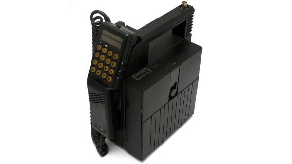
The SDR revolution has completely changed the way radio enthusiasts pursue their hobby, but there is still a space for the more traditional scanning receiver. If you are an American, have you ever noticed that it has a gap in its coverage between 800 and 900 MHz? The curious reason for this is explored by [J. B. Crawford], and it’s a tale of dusty laws relating to a long-gone technology, remaining on the books only because their removal requires significant political effort.

What we might today refer to as “1G” phones used an entirely analogue transmission scheme, with an easily-receivable FM carrier for the voice and extremely low-bandwidth bursts of serial data only for the purposes of managing the call. Listening to these calls was an illegal activity, but for those with the appropriate scanners it became a voyeuristic hobby within a hobby. It even made the world news via the pages of the gossip sheets, when (truthfully or not) it was credited for the leak of a revealing and controversial conversation involving Diana Princess of Wales.

This caused significant worry to the cellular phone companies who understandably didn’t want their product to become associated with insecurity. Thus they successfully petitioned the US Congress to include a clause restricting the capabilities of scanning receivers into another telecoms-related Act, and here we are three decades later with analogue phones a distant memory and the law still on the books. It may be ancient and unnecessary but there is neither the will nor the resources to remove it, so it seems destined to become one of those curious legal oddities that remains on the books for centuries. Whether an RTL-SDR breaks it is something we’ll leave for the lawyers, but the detail in the write-up makes it well worth a read.

Header image: krystof.k (Twitter) & nmuseum, CC BY-SA 3.0.

Bringing Full Colour PCB Art To Production

One of the Holy Grails in the world of electronic badges has been full-colour PCB art as a logical progression from the limited palette of traditional PCB artwork. In the progression towards achieving this goal there have been a variety of techniques applied, and it’s become an expensive commercial possibility rather than an unachievable dream. Has it become practical for mere mortals then? [Tom Clement] has put together a write-up of his progression towards achieving full-colour PCB artwork on a limited production run , and it makes for a fascinating read.

The board in question is the Pixel badge, an improved commercial version of the CampZone 2019 I-Pane badge we reviewed last year. It’s a very bright large multicolour LED matrix that has caught the eye of campgoers at events ever since the original, and has generated enough demand for a new production run. As well as a few electronic enhancements it replaces the original’s dithered monochrome silkscreen rear art with a full-colour design, and it is that with which the write-up is concerned.

It starts with UV printing, and goes through the various iterations of the process until a satisfactory result is achieved. We learn about the effect of reflow temperatures on UV printing inks, it seems that white ink discolours with temperature and the inventive solution is to transfer all the whites to the PCB silkscreen layer. He closes with a discourse on alignment, and we start to appreciate the achievement behind producing this badge. A colour print isn’t necessary for the Pixel’s eye-searing light show, but the point of badges is as much to show off the cutting edge of the art.

As the regular Hackaday reader will know, colour PCB art is a long-time topic of interest here at Hackaday.

A SNES, Ray Tracing

A trick famously used by Nintendo to keep its slowly aging SNES console fresh against newer competition was to produce new games with extra support chips in the cartridge to push out hitherto-unthinkable performance. Chips such as the famous SuperFX gave us 3D polygonal graphics, but it would have been a few more years before even much faster platforms could achieve real-time ray-tracing. Nintendo may not have managed it, but here in 2020 [Ben Carter] has a SNES on his bench rendering a complex 3D ray-traced world.

Ray tracing refers to the practice of rendering a scene with accurate lighting by tracing the rays of light that go towards making each pixel. It can achieve results that even approach photorealism, but it remains an extremely computationally intensive job for any computer. To do this with a SNES he hasn’t resorted to a modern computer like the excellent Raspberry-Pi-based NES DOOM cartridge, instead he’s tried to create something that might have graced a Nintendo custom chip back in the 1990s. The tool may be a thoroughly modern DE10-Nano FPGA dev board, but what it implements could conceivably have been made as a 1990s-spec ASIC. In it are three ray tracing cores that do the work, but the final rendering is handled by the SNES itself. At 200 x 160 pixels and 256 colours it’s no graphical powerhouse, but the maximum frame rate of 30 fps makes it no slouch for the day. The video below the break supplies extra detail.

Perhaps an unexpected takeaway of the rendered scene lies in how of its era it seems. It comes from an age in which checker-board floors, mirrored balls, and azure blue skies looked so futuristic, and just before the likes of Toy Story redefined what the general public might expect from 3D rendering. If Nintendo had produced a ray-traced SNES game using a chip like this one, it would have certainly been a defining moment for gaming in that decade.

Continue reading “A SNES, Ray Tracing”

Teardown: Siemens 8mm SMD Parts Feeder

Many of Hackaday’s readers will be no stranger to surface mount electronic components, to the extent that you’ll likely be quite comfortable building your own surface-mount projects. If you have ever built a very large surface-mount project, or had to do a number of the same board though, you’ll have wished that you had access to a pick-and-place machine. These essential components of an electronics assembly line are CNC robots that pick up components from the reels of tape in which they are supplied, and place them in the appropriate orientation in their allotted places on the PCB. They are an object of desire in the hardware hacker community and over the years we’ve seen quite a few home-made examples. Their workings are easy enough to understand, but there is still much to gain by studying them, thus it was very interesting indeed to see a friend acquiring a quantity of surplus Siemens component feeders from an older industrial pick-and-place machine. A perfect opportunity for a teardown then, to see what makes them tick.

Continue reading “Teardown: Siemens 8mm SMD Parts Feeder”

Auto Tuning For A Vintage Stereo

In 1984 there weren’t many ways to listen to high-quality music, so an FM tuner was an essential part of any home hi-fi system. The Pioneer TX-950 picked up by [The Curious Lorenz] would have been someone’s pride and joy, with its then-cutting-edge microprocessor control, digital PLL tuning, and seven-segment displays. Astoundingly it doesn’t have an auto-tuning function though, so some work to implement the feature using an ATtiny85 was called for.

A modern FM tuner would be quite likely to use an all-in-one tuner chip using SDR technology under the hood, but this device from another era appears to be a very conventional analog tuner to which the PLL and microprocessor have been grafted. There are simple “Up” and “Down” buttons and a “Station tuned” light. One might imagine that given these the original processor could have done autotune. At least the original designers were kind enough to provide the ATtiny with the interfaces it needs. Pressing either button causes it to keep strobing its line until the “Station tuned” line goes high, at which point it stops. It’s an extremely simple yet effective upgrade, and since the ATtiny is so small it’s easily placed on top of the original PCB. The result is an ultra-modern tuner from 1984, that’s just that little bit more modern than it used to be.

If you don’t have a vintage FM radio, you can always build its modern equivalent.

A 3D – To – 2D Converter To Make Plots From STLs.

We’ve become used to finding models on websites such as Thingiverse and downloading them to print. After all, whose hackerspace doesn’t have a pile of novelty prints? How about printing them on paper? For the plotter enthusiast that can be particularly annoying. Never fear, [Trammell Hudson] is here with an online 3D to 2D converter just for plotters. [Trammell’s] creation makes a vector image suitable for a plotter while eliminating spurious behind-the-scenes lines.

Plotter drawings are the pen-and-paper equivalent of a vector CRT display, in which the graphics are printed as continuous strokes. Rendering a 3D model as a wireframe for a plotter requires the removal of any pen strokes that comes from the 3D space behind the surface in view. Loading various models into the web page seemed to do a pretty good job of this, though the ubiquitous Benchy 3d printer test model lived up to its billing as a torture test in taking several minutes to render.

As anyone who has followed the #PlotterTwitter social media hashtag will know, there is a considerable community of pen plotter enthusiasts who are pushing the boundaries of what their machines can do. [Trammell] has posted his plotter producing some of the work created with this tool, and we can see that it’s likely to work better with lower-poly models.

We’ve featured a lot of plotters over the years as they seem to be a popular project. If you’d like one then they can be made from the most available parts, including those scavenged from scrap DVD drives, or printers.

Still Got Film To Scan? This Lego And Raspberry Pi Scanner Is For You

There was a time during the early years of mass digital photography, when a film scanner was a common sight. A small box usually connected to a USB port, it had a slot for slides or negatives. In 2020 they’reĀ  a rare breed, but never fear! [Bezineb5] has a solution in the shape of an automated scanner using a Radpberry Pi and a mechanism made of Lego.

The Lego mechanism is a sprocket feeder that moves the film past the field of view from an SLR camera. The software on the Pi runs in a Docker container, and features a machine learning approach to spotting frame boundaries. This is beyond the capabilities of the Pi, so is offloaded to a Google Coral accelerator.

The whole process is automated with the Pi controlling not only the Lego but also the camera, to the extent of retrieving the photos from it to the Pi. There’s a smart web interface to control everything, making the process — if you’ll excuse the pun — a snap. There’s a video of it in action, that you can see below the break.

We’ve featured many film scanner projects over the years, one that remains memorable is this 3D printed lens mount.

Continue reading “Still Got Film To Scan? This Lego And Raspberry Pi Scanner Is For You”