Soldering Holder From Old Lamps

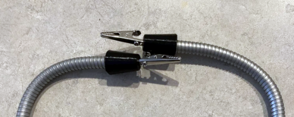
One of the neat things about 3D printing is that you can create custom parts to fit salvage to use in projects. For example, [Willyrags05] took a lamp — looks like something you might find at a resale shop — harvested the gooseneck tubes from it.

Before 3D printing, it would have required ingenuity to cobble together some way to secure base and add a clamp to the other end. A blob of epoxy wouldn’t look as nice and not everyone can machine nice round adapters. Don’t have the same lamp? No problem. You can easily modify the adapters or create new ones to print for yourself.

Outside of the 3D printer, the project required a way to cut the ends off the tubes. [Willy] used a chop saw, but it seems like a hacksaw or bolt cutters might work. Neatness doesn’t count since the printed adapter will cover all sins.

Once the tubes are ready, some glue, magnets, and alligator clips (why aren’t these crocodile clips?) complete the assembly. [Willy] mentions he needs stronger magnets, but we might have been tempted to make the bases wider with depressions for multiple magnets. This is probably a project you won’t duplicate exactly, but it may well inspire you to upcycle that old lamp in the attic.

Maybe you prefer a vise-like holder. There are plenty of other choices.

The decapped chip on top of some other DIP IC, with magnet wire soldered to the die, other ends of the magnet wire soldered to pins of the "body donor" DIP IC.

Factory Defect IC Revived With Sandpaper And Microsoldering

We might be amidst a chip shortage, but if you enjoy reverse-engineering, there’s never a shortage of intriguing old chips to dig into – and the 2513N 5×7 character ROM is one such chip. Amidst a long thread probing a few of these (Twitter, ThreadReader link), [TubeTime] has realized that two address lines were shorted inside of the package. A Twitter dopamine-fueled quest for truth has led him to try his hand at making the chip work anyway. Trying to clear the short with an external PSU led to a bond wire popping instead, as evidenced by the ESD diode connection disappearing.

A dozen minutes of sandpaper work resulted in the bare die exposed, making quick work of the bond wires as a side effect. Apparently, having the bond pads a bit too close has resulted in a factory defect where two of the pads merged together. No wonder the PSU wouldn’t take that on! Some X-acto work later, the short was cleared. But without the bond wires, how would [TubeTime] connect to it? This is where the work pictured comes in. Soldering to the remains of the bond wires has proven to be fruitful, reviving the chip enough to continue investigating, even if, it appears, it was never functional to begin with. The thread continued on with comparing ROMs from a few different chips [TubeTime] had on hand and inferences on what could’ve happened that led to this IC going out in the wild.

Such soldering experiments are always fun to try and pull off! We rarely see soldering on such a small scale, as thankfully, it’s not always needed, but it’s a joy to witness when someone does IC or PCB microsurgery to fix factory defects that render our devices inoperable before they were even shipped. Each time that a fellow hacker dares to grind the IC epoxy layers down and save a game console or an unidentified complex board, the world gets a little brighter. And if you aren’t forced to do it for repair reasons, you can always try it in an attempt to build the smallest NES in existence!

Continue reading “Factory Defect IC Revived With Sandpaper And Microsoldering”

BGA Hand Soldering Uses Tombstone Resistor Technique, Demands Surgical Precision

Most Hackaday readers will be a pretty dab hand with a soldering iron. We can assemble surface-mount boards, SOICs and TSSOPs are a doddle, 0402s we take in our stride, and we laugh in the face of 0201s. But a Twitter thread from [Greg Davill] will probably leave all but the most hardcore proponents of the art floundering, as he hand-wires a tiny FPGA in a BGA package to the back of a miniature dot-matrix LED display module.

Resistors soldered on-end, awaiting wires to connect to the BGA microcontroller

As far as we can see the module must once have had its own microcontroller which has been removed. We’d guess it was under an epoxy blob but can’t be sure, meanwhile its pads are left exposed. The Lattice LP1k49 fits neatly into the space, but a web of tiny wires are required to connect it to those pads. First, [Greg] populates the pads with a set of “tombstoned” tiny (we’re guessing 0R) resistors, then wires them to the pads with 30μm wire. He describes a moment of confusion as he attempts to tin a stray hair, which burns rather than accepting the solder.

The result is a working display with a new brain, which surprises even him. We’ve seen more than one BGA wiring over the years, but rarely anything at this scale.

It’s worth mentioning that [Greg] was behind the FLIR frame grabber that was a runner-up in last year’s Hackaday Prize. We admire the photos he’s able to get of all of his projects and aspire to reach this level with our own. Take this as inspiration and then check out the Hackaday contest for Beautiful Hardware images happening right now.

Thanks [Sophi] for the tip.

Fail Of The Week: When The Epoxy-Coated Chip Is Conductive

Every once in a while, you’ll find some weirdness that will send your head spinning. Most of the time you’ll chalk it up to a bad solder joint, some bad code, or just your own failings. This time it’s different. This is a story of weirdness that’s due entirely to a pin that shouldn’t be there. This is a package for an integrated circuit that has a pin zero.

The story begins with [Erich] building a few development boards for the Freescale Kinetis K20 FPGA. This is a USB-enabled microcontroller, and by all accounts, a worthwhile effort. So far, so good. The problem with the prototype boards was soon apparent. On some of the boards, the external 32 kHz oscillator was not starting. Resoldering the oscillator or microcontroller sometimes solved the problem, but not always. This is troubling, because that means the issue isn’t code, and it’s not the PCB. This is going to take a deep dive and a good inspection microscope.

One of [Erich]’s friends, [Christian B] somehow found the problem. When the Freescale K40 is manufactured, the die is carefully laid in a chip carrier and coated with epoxy, putting it in a small QFN package. The problem is, there’s an extra connection sticking out of one corner of this chip. This is just an artifact of the chip carrier, but if you leave exposed metal connected to ground, something is eventually going to go wrong.

The best guess [Erich] has is that this additional connection is from the manufacturing and packaging process, with the exposed metal pad in this application being bridged to an adjacent pad. Now, if there’s one failure to [Erich]’s design, it’s that the trace comes out of the pin on the adjacent pad at 90 degrees; this isn’t a best practice, but most of the time you can get away with it. This time, though, somebody got burned.

We don’t know how [Christian] ever found this issue. When you look at a tiny QFN package, you don’t expect there to be an extra pin attached to ground that can be easily bridged with a bit of solder paste. It’s either a lot of luck or skill to find this problem, but it’s a great example of the weird things you have to look out for.

Epoxy Fix For A Combusted PCB

When the Magic Smoke is released, chances are pretty good that you’ve got some component-level diagnosis to do. It’s usually not that hard to find the faulty part, charred and crusty as it likely appears. In that case, some snips, a new non-crusty part, and a little solder are usually enough to get you back in business.

But what if the smoke came not from a component but from the PCB itself? [Happymacer] chanced upon this sorry situation in a power supply for an electric gate opener. Basking in the Australian sunshine for a few years, the opener started acting fussy at first, then not acting at all. Inspection of its innards revealed that some unlucky ants had shorted across line and neutral on the power supply board, which burned not only the traces but the FR4 of the board as well. Rather than replace the entire board, [Happymacer] carefully removed the carbonized (and therefore conductive) fiberglass and resin, leaving a gaping hole in the board. He fastened a patch for the hole from some epoxy glue; Araldite is the brand he used, but any two-part epoxy, like JB Weld, should work. One side of the hole was covered with tape and the epoxy was smeared into the hole, and after a week of curing and a little cleanup, it was ready for duty. The components were placed into freshly drilled holes, missing traces were replaced with wire, and it seems to be working fine.

This seems like a great tip to keep in mind for when catastrophe strikes your boards. There are more extreme ways to do it, of course, but perhaps none so flexible. After all, epoxy is versatile stuff.

PCB Solder Pad Repair & Cleanup

What do you do when your motherboard is covered in electrolytic grime, has damaged pads and traces that are falling apart? You call [RetroGameModz] to work their magic with epoxy and solder.

While this video is a bit old, involved repair videos never go out of style. What makes this video really special is that it breaks from the common trend of “watch me solder in silence” (or it’s close cousin, “watch me solder to loud music”). Instead, [RetroGameModz] walks you through what they’re doing, step by step in their repair of a motherboard. And boy do they have their work cut out for them: the motherboard they’re working on has definitely seen better days. Specifically, it was better before corrosion from a leaking electrolytic capacitor and the well-meaning touch of its owner.

After a quick review of the damage, all of the components are removed from the battle zone. Then the cleaning begins, taking special precautions not to rip pads up. After everything’s cleaned up, things get really interesting. [RetroGameModz] starts to make their own pads from raw copper using the old pads as templates to replace the missing ones on the motherboard. After a bit of epoxy, it’s hard to tell that the pads were handmade, they fit in so well.

This epoxy trick is also used to deal with some heavily damaged traces, cool! During this repair, [RetroGameModz] used an epoxy that is heat resistant up to 315°C for 60 seconds. If you ever find any kind of epoxy on the market that is specified to be heat resistant up to more than 315°C, [RetroGameModz] would be quite happy if you could leave some info in the comment section, as they’ve found high-temperature epoxies quite difficult to source.

This goes to show that some repairs really should be done by professionals. [RetroGameModz] surely agrees, stating that “If you are not a repair technician and your motherboard has stopped working, it would be in the best of your own interest not to attempt a repair that you really cannot handle.” Good advice. But, we can never resist trying to fix things ourselves before handing things off to the more experienced. Call it a vice, or a virtue; we’ll call it fun.

What do you think? Are there some repairs you rely on technicians for? Or do you fix everything yourself? Let us know in the comments.

Continue reading “PCB Solder Pad Repair & Cleanup”

Solder Paste Dispenser Has No 3D Printed Parts!

If you’ve never used a solder paste dispenser, you’re missing out. Think about always using a crappy soldering iron, and then for the first time using a high-end one. Suddenly you’re actually not bad at soldering things! It’s kind of like that.

Most solder paste dispensers make use of compressed air, which requires an extra setup to use that you might not have. The goal of this project was to make a solder paste dispenser that doesn’t use compressed air, and doesn’t have any 3D printed parts (in case you don’t have a 3D printer) — and it looks like the inventor, [MikeM], succeeded!

Continue reading “Solder Paste Dispenser Has No 3D Printed Parts!”