A few years ago, [Smashcat] ported a ZX Spectrum game called Manic Miner to the Arduino Uno. The Arduino has less memory than the original Spectrum did, so doing all this on an 8-bit microcontroller was no easy lift. Since then, parts of this original port have been adapted to produce a game engine, allowing [Smashcat] to port several other games to the Arduino Uno as well.
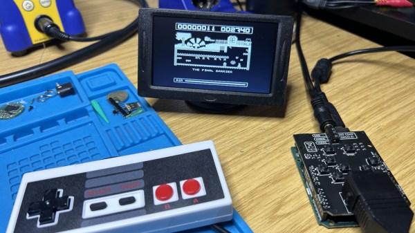
The engine is able to host a 2D map with the ability to scroll, at a resolution of 256×256, as well as up to nine sprites at the same time. The graphics are locked to 50 FPS, but only with a real Arduino Uno that has a crystal oscillator. Some replica boards do not have a timekeeping chip accurate enough to replicate the video signal, which is done without a framebuffer. That signal, as well as two PWM audio channels, are still generated directly as well, with only a few resistors needed to hook everything up to a monitor and a controller, including the option of using an NES controller.
With all of that running on the Arduino and it hooked up to the daughterboard that provides the controller interface as well as the resistors for the video signal to function and a driver for a speaker, the system now runs the original Manic Miner as well as three other games: Scramble, Space Invaders, and Pac Man.
The engine and the rest of the code are available on a GitHub page as well, and there’s even a WebAssembly version available to run various pieces of the software without the specific hardware. The original ZX Spectrum was an interesting machine too that still inspires builds like this, despite it being well over 40 years old now.