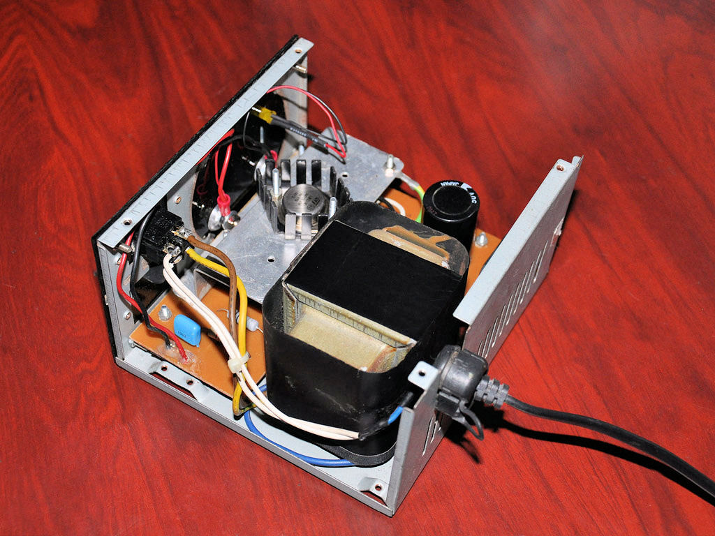
After years of seeing people showing off and trading their badge Simple Add-Ons (SAOs) at Supercon, this year I finally decided to make one myself. Now for a first attempt, it would have been enough to come up with some cool PCB art and stick a few LEDs on it. But naturally I started with a concept that was far more ambitious than necessary, and before long, had convinced myself that the only way to do the thing justice was to have an onboard microcontroller.
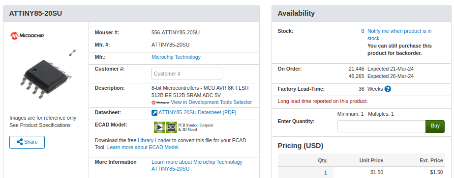
My first thought was to go with the venerable ATtiny85, and since I already had a considerable stock of the classic eight-pin DIP MCUs on hand, that’s what I started prototyping with. After I had something working on the breadboard, the plan was to switch over to the SOIC-8 version of the chip which would be far more appropriate for something as small as an SAO.
Unfortunately, that’s where things got tricky. I quickly found that none of the major players actually had the SMD version of the chip in stock. Both DigiKey and Mouser said they didn’t expect to get more in until early 2024, and while Arrow briefly showed around 3,000 on hand, they were all gone by the time I checked back. But that was only half the problem — even if they had them, $1.50 a piece seems a hell of a lot of money for an 8-bit MCU with 8K of flash in 2023.
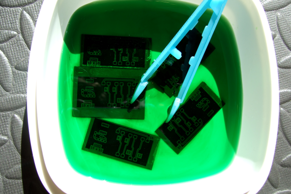
The whole thing was made all the more frustrating by the pile of DIP8 ATtiny85s sitting on the bench, mocking me. Under normal circumstances, using them in an SAO wouldn’t really be a problem, but eight hand-soldered leads popping through the front artwork would screw up the look I had in mind.
While brooding over the situation my eyes happened to fall on one of the chips I had been fiddling with, it’s legs badly bent from repeated trips through the programmer. Suddenly it occurred to me that maybe there was a way to use the parts I already had…
Continue reading “Chip Shortage Engineering: Misusing DIP Packages”
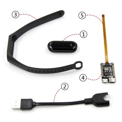 In this article, let’s figure out places where you can use a logic analyzer, and places where you can’t. We’ll start with the first limitation of logic analyzers – capture speed. For instance, here’s a cool thing you can buy on Aliexpress – a wristband from TTGO that looks like a usual fitness tracker, but has an ESP32 in it, together with an IMU, an RTC, and an IPS screen! The seller also has an FFC-connectable devboard for programming this wristband over UART, plus vibromotor and heartrate sensor expansion modules.