By now you’ve doubtless heard that the FBI has broken the encryption on Syed Farook — the suicide terrorist who killed fourteen and then himself in San Bernardino. Consequently, they won’t be requiring Apple’s (compelled) services any more.
A number of people have written in and asked what we knew about the hack, and the frank answer is “not a heck of a lot”. And it’s not just us, because the FBI has classified the technique. What we do know is that they paid Cellebrite, an Israeli security firm, at least $218,004.85 to get the job done for them. Why would we want to know more? Because, broadly, it matters a lot if it was a hardware attack or a software attack.
We have talked about a whole slew of logic and interconnect technologies including TTL, CMOS and assorted low voltage versions. All of these technologies have in common the fact that they are single-ended, i.e. the signal is measured as a “high” or “low” level above ground.
This is great for simple uses. But when you start talking about speed, distance, or both, the single ended solutions don’t look so good. To step in and carry the torch we have Differential Signalling. This is the “DS” in LVDS, just one of the common standards throughout industry. Let’s take a look at how differential signaling is different from single ended, and what that means for engineers and for users.
Single Ended
Single Ended: TTL, CMOS, LVTTL, Etc.
Single Ended and Sources of Noise
Collectively, standards like TTL, CMOS, and LVTTL are known as Single Ended technologies and they have in common some undesirable attributes, namely that ground noise directly affects the noise margin (the budget for how much noise is tolerable) as well as any induced noise measured to ground directly adds to the overall noise as well.
By making the voltage swing to greater voltages we can make the noise look smaller in proportion but at the expense of speed as it takes more time to make larger voltage swings, especially with the kind of capacitance and inductance we sometimes see.
Differential
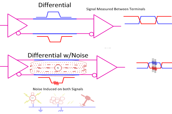
Enter Differential Signaling where we use two conductor instead of one. A differential transmitter produces an inverted version of the signal and a non-inverted version and we measure the desired signal strictly between the two instead of to ground. Now ground noise doesn’t count (mostly) and noise induced onto both signal lines gets canceled as we only amplify the difference between the two, we do not amplify anything that is in common such as the noise.
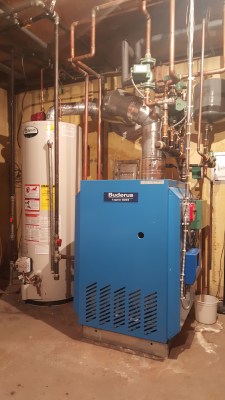
It’s been said that hackers are enamored with complex networks. In the 60s and 70s, the telephone network was the biggest around, singing a siren song to an entire generation of blue-boxing phone phreaks. I started a bit closer to the house. As a child I was fascinated by the heating system in the basement of our home: a network of pipes with a giant boiler in the middle. It knew when to come on to provide heat, and when to kick on for hot water. I spent hours charting the piping and electrical inputs and outputs, trying to understand how everything worked. My parents still tell stories of how I would ask to inspect the neighbors heating systems. I even pestered the maintenance staff at my nursery school until they finally took me down to see the monstrous steam boiler which kept the building warm.
My family was sure I would grow up to be a Heating Ventilation and Air Conditioning (HVAC) tech. As it turned out, electronics and embedded systems were my calling. They may not have been too far from the truth though, as these days I find myself designing systems for a major manufacturer of boiler controls and thermostats.
Recently a house hunt led me to do some HVAC research on the web. What I found is that HVAC techs have created a great community on the internet. Tradesmen and women from all over the world share stories, pictures, and videos on websites such as HVAC-Talk and HeatingHelp.
A very good question came up on The EEVBlog forum that I thought deserved an in depth answer. The poster asked why would amplifier companies in the heyday of tube technology operate tubes in mass produced circuits well in excess of their published manufacturers recommended limits. The simple answer is: because the could get away with it. So the real question worth exploring is how did they get away with operating outside of their own published limitations? Let’s jump in and take a look at the collection of reasons.
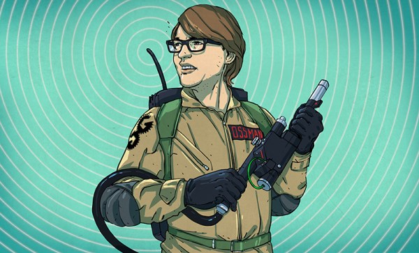
To a lot of people, radio-frequency (RF) design is black magic. Even if you’ve built a number of RF projects, and worked your way through the low-lying gotchas, you’ve probably still got a healthy respect for the gremlins lying in wait around every dimly-lit corner. Well, [Michael Ossmann] gave a super workshop at the Hackaday Superconference to give you a guided tour of the better-illuminated spaces in RF design.
[Michael] is a hacker-designer, and his insights into RF circuit design are hard-won, by making stuff. The HackRF One is probably his most famous (and complex) project, but he’s also designed and built a number of simpler RF devices. And the main point of his talk is that there’s a large range of interesting projects that are possible without getting yourself into the fringes of RF design (which require expensive test equipment, serious modelling, or a Ph.D. in electro-wavey-things).
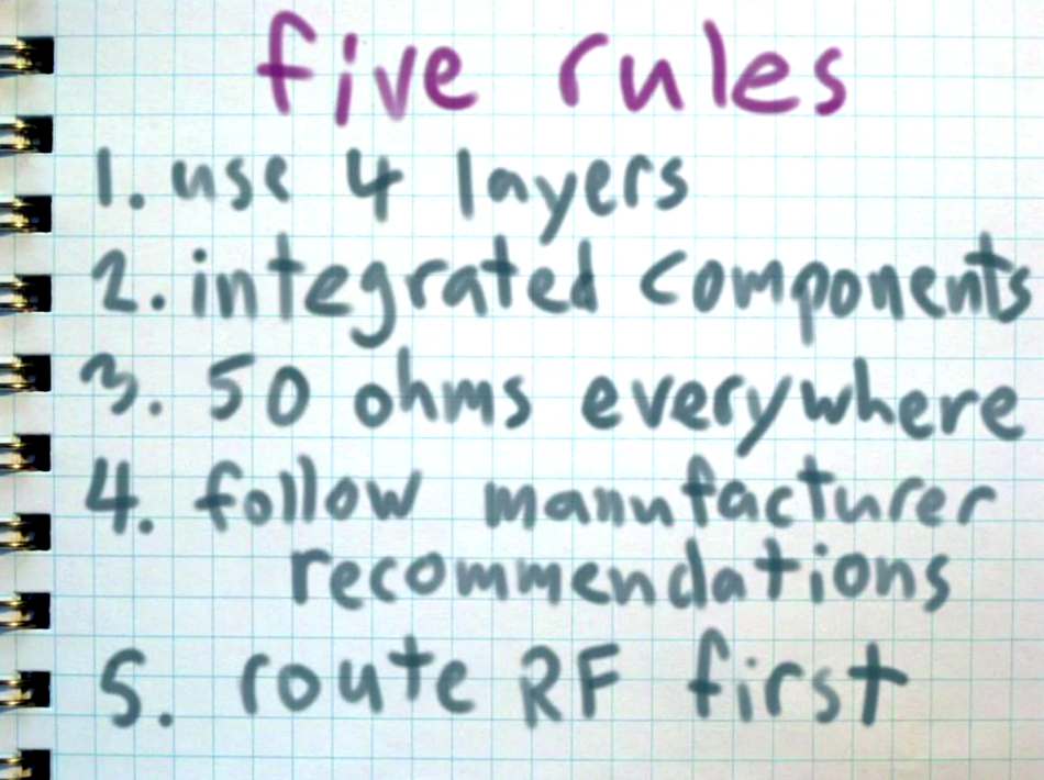
You should watch [Mike]’s workshop which is embedded below. That said, here’s the spoilers. [Mike] suggests five rules that’ll keep your RF design on the green, rather than off in the rough.
If you want a stable oscillator, you usually think of using a crystal. The piezoelectric qualities of quartz means that it can be cut in a particular way that it will oscillate at a very precise frequency. If you present a constant load and keep the temperature stable, a crystal oscillator will maintain its frequency better than most other options.
There are downsides to crystals, though. As you might expect, because crystals are so stable it’s hard to change the frequency much when you want a different one. You can use a trimming capacitor to pull the frequency a little, but to really change frequency, you have to change crystals.
There are other kinds of oscillators that are more frequency agile. However, they aren’t usually as stable. To combine flexibility with crystal-like stability, you can use a Phase Locked Loop (PLL). Many modern systems use direct digital synthesis, but the PLL is a venerable and time-tested technique.
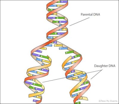
Our bodies rely on DNA to function, it’s often described as “the secret of life”. A computer program that describes how to make a man. However inaccurate these analogies might be, DNA is fundamental to life. In order for organisms to grown and replicate they therefore need to copy their DNA.
Since the discovery of its structure in 1953, the approximate method used to copy DNA has been obvious. The information in DNA is encoded in 4 nucleotides (which in their short form we call A,T,G, and C). These couple with each other in pairs, forming 2 complimentary strands that mirror each other. This structure naturally lends itself to replication. The two strands can dissociate (under heat we call this melting), and new strands form around each single stranded template.
However, this replication process can’t happen all by itself, it requires assistance. And it wasn’t until we discovered an enzyme called the DNA polymerase that we understood how this worked. In conjunction with other enzymes, double stranded DNA is unwound into 2 single strands which are replicated by the polymerase.




 It’s been said that hackers are enamored with complex networks. In the 60s and 70s, the telephone network was the biggest around, singing a siren song to an entire generation of blue-boxing phone phreaks. I started a bit closer to the house. As a child I was fascinated by the heating system in the basement of our home: a network of pipes with a giant boiler in the middle. It knew when to come on to provide heat, and when to kick on for hot water. I spent hours charting the piping and electrical inputs and outputs, trying to understand how everything worked. My parents still tell stories of how I would ask to inspect the neighbors heating systems. I even pestered the maintenance staff at my nursery school until they finally took me down to see the monstrous steam boiler which kept the building warm.