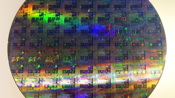
FPGAs are somewhat the IPv6 of integrated circuits — they’ve been around longer than you might think, they let you do awesome things that people are intrigued by initially, but they’ve never really broke out of their niches until rather recently. There’s still a bit of a myth and mystery surrounding them, and as with any technology that has grown vastly in complexity over the years, it’s sometimes best to go back to its very beginning in order to understand it. Well, who’d be better at taking an extra close look at a chip than [Ken Shirriff], so in his latest endeavor, he reverse engineered the very first FPGA known to the world: the Xilinx XC2064.
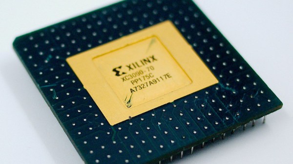
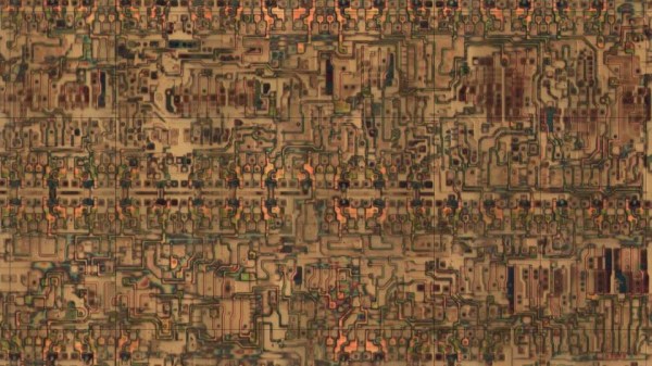
If you ever wished for a breadboard-friendly FPGA, the XC2064 can scratch that itch, although with its modest 64 configurable logic blocks, there isn’t all that much else it can do — certainly not compared to even the smallest and cheapest of its modern successors. And that’s the beauty of this chip as a reverse engineering target, there’s nothing else than the core essence of an FPGA. After introducing the general concepts of FPGAs, [Ken] (who isn’t known to be too shy to decap a chip in order to look inside) continued in known manner with die pictures in order to map the internal components’ schematics to the actual silicon and to make sense of it all. His ultimate goal: to fully understand and dissect the XC2064’s bitstream.
Of course, reverse engineering FPGA bitstreams isn’t new, and with little doubt, building a toolchain based on its results helped to put Lattice on the map in the maker community (which they didn’t seem to value at first, but still soon enough). We probably won’t see the same happening for Xilinx, but who knows what [Ken]’s up to next, and what others will make of this.