Problem: your electronic load works fine, except for the occasional MOSFET bursting into flames. Solution: do what [tbladykas] did, and build a water-cooled electronic load.
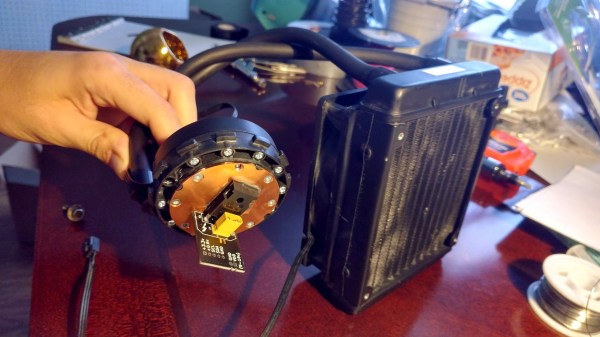
One can quibble that perhaps there are other ways to go about preventing your MOSFETs from burning, including changes to the electrical design. But he decided to take a page from [Kerry Wong]’s design book and go big. [Kerry]’s electronic load was air-cooled and capable of sinking 100 amps; [tbladykas] only needed 60 or 70 amps or so. Since he had an all-in-one liquid CPU cooler on hand, it was only natural to use that for cooling.
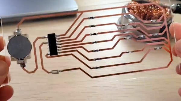
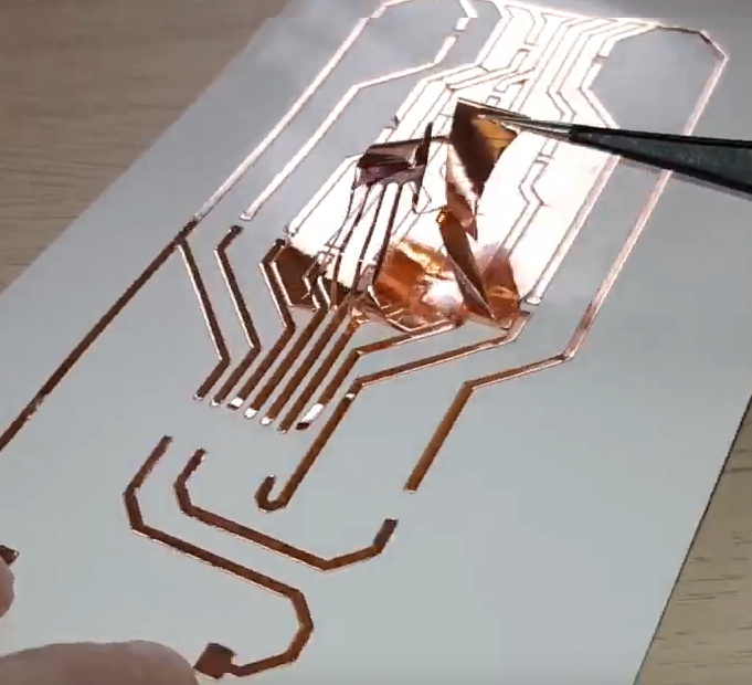
The IXYS linear MOSFET dangles off the end of the controller PCB, where the TO-247 device is soldered directly to the copper cold plate of the AiO cooler. This might seem sketchy as the solder could melt if things got out of hand, but then again drilling and tapping the cold plate could lead to leakage of the thermal coupling fluid. It hasn’t had any rigorous testing yet – his guesstimate is 300 Watts dissipation at this point – but as his primary endpoint was to stop the MOSFET fires, the exact details aren’t that important.
We’ve seen a fair number of liquid-cooled Raspberry Pis and Arduinos before, but we can’t find an example of a liquid-cooled electronic load. Perhaps [tbladykas] is onto something with this design.