Four M.2 cards of different sizes on a desk surface

M.2 For Hackers – Cards

Last time, I’ve explained everything you could want to know if you wanted to put an M.2 socket onto your board. Today, let’s build M.2 cards! There’s a myriad of M.2 sockets out there that are just asking for a special card to be inserted into it, and perhaps, it’s going to be your creation that fits.

Why Build Cards?

Laptops and other x86 mainboards often come with M.2 slots. Do you have a free B-key slot? You can put a RP2040 and bunch of sensors on a B-key PCB as an experimental platform carried safely inside your laptop. Would you like to do some more advanced FPGA experiments? Here’s a miniscule FPGA board that fits inside your laptop and lets you play with PCIe on this same laptop – the entire setup having a super low footprint. Are you looking for an extra PCIe link because you’re reusing your laptop as a home server? Again, your WiFi slot will provide you with that. Want to get some PCIe out of a SteamDeck? Building a M-key 2230 card seems to be your only hope! Continue reading “M.2 For Hackers – Cards”

M.2 For Hackers – Connectors

In the first M.2 article, I’ve described real-world types and usecases of M.2 devices, so that you don’t get confused when dealing with various cards and ports available out there. I’ve also designed quite a few M.2 cards and card-accepting adapters myself. And today, I’d like to tell you everything you need to know in order to build M.2 tech on your own.

There’s two sides to building with M.2 – adding M.2 sockets onto your PCBs, and building the PCBs that are M.2 cards. I’ll cover both of these, starting with the former, and knowing how to deal with M.2 sockets might be the only thing you ever need. Apart from what I’ll be describing, there’s some decent guides you can learn bits and pieces from, like the Sparkfun MicroMod design guide, most of which is MicroMod-specific but includes quite a few M.2 tips and tricks too.

First, Let’s Talk About The Y-Key

What could you do with a M.2 socket on your PCB? For a start, many tasty hobbyist-friendly SoMs and CPUs now have a PCIe interface accessible, and if you’re building a development board or a simple breakout, an M.2 socket will let you connect an NVMe SSD for all your high-speed low-power storage needs – many Raspberry Pi Compute Module mainboards have M.2 M-key sockets specifically for that, and there’s NVMe support in the RPi firmware to boot. Plus, you can always plug a full-sized PCIe adapter or an extender into such a socket and connect a PCIe network card or other much-needed device – even perhaps, an external GPU! However, as much as PCIe-equipped SoMs are tasty, they’re far from the only reason to use M.2 sockets.

Continue reading “M.2 For Hackers – Connectors”

PCB antenna rendered useless by overly enthusiastic copper fill.

The Many Ways You Can Easily Ruin Your PCB Antenna Design

PCB antenna impaired by copper fill and other attenuation sources.

We have all seen Printed Circuit Board (PCB) antennas: those squiggly bits of traces on PCBs connected often to a Bluetooth, WiFi or other wireless communication chip. On modules like for the ESP8266 and ESP32 platforms the PCB antennas are often integrated onto the module’s PCB, yet even with such a ready-made module it’s possible to completely destroy the effectiveness of this antenna. These and other design issues are discussed in this article by [MisterHW].

It covers a range of examples of poor design, from having ground fill underneath an antenna, to having metal near the antenna, to putting dielectric materials near or on top of the antenna. The effect of all of these issues is generally to attenuate the signal, sometimes to the point where the antenna is essentially useless.

Ultimately, the best PCB antenna design is one where there is no nearby copper fill, and there are no traces running near or on layers below the antenna. After all, any metal trace or component is an antenna, and any dielectric materials will dampen the signal. Fortunately, there is e.g. a free KiCad library with ready-to-use PCB antenna designs to help one get started with a custom design, as well as many other resources, covered in the article.

If you want to get really professional about checking the effectiveness of an antenna design, you’ll want to use a Network Vector Analyzer. These will also help you with tuning the capacitors used with the PCB antenna.

(Featured image: PCB antenna rendered useless by overly enthusiastic copper fill.)

The Meraki AP PCB on a desk, case-less, with three USB-UARTs connected to its pins - one for interacting with the device, and two for monitoring both of the UART data lines.

Flashing Booby-Trapped Cisco AP With OpenWrt, The Hard Way

Certain manufacturers seriously dislike open-source firmware for their devices, and this particular hack deals with quite extreme anti-hobbyist measures. The Meraki MR33, made by Cisco, is a nice access point hardware-wise, and running OpenWrt on it is wonderful – if not for the Cisco’s malicious decision to permanently brick the CPU as soon as you enter Uboot through the serial port. This AP seems to be part of a “hardware as a service” offering, and the booby-trapped Uboot was rolled out by an OTA update some time after the OpenWrt port got published.

There’s an older Uboot version available out there, but you can’t quite roll back to it and up to a certain point, there was only a JTAG downgrade path noted on the wiki – with its full description consisting of a “FIXME: describe the process” tag. Our hacker, an anonymous user from the [SagaciousSuricata] blog, decided to go a different way — lifting, dumping and modifying the onboard flash in order to downgrade the bootloader, and guides us through the entire process. There’s quite a few notable things about this hack, like use of Nix package manager to get Python 2.7 on an OS which long abandoned it, and a tip about a workable lightweight TFTP server for such work, but the flash chip part caught our eye.

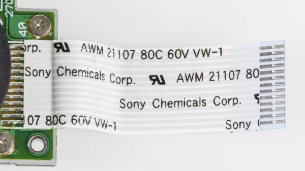
The flash chip is in TSOP48 package and uses a parallel interface, and an iMX6.LL devboard was used to read, modify and flash back the image — hotswapping the chip, much like we used to do with old parallel-interface BIOS chips. We especially liked the use of FFC cables and connectors for connecting the flash chip to the devboard in a way that allows hotswapping – now that we can see it, the TSOP 0.5 mm pitch and 0.5 mm FFC hardware are a match made in heaven. This hack, of course, will fit many TSOP48-equipped devices, and it’s nice to have a toolkit for it in case you don’t have a programmer handy.

In the end, the AP got a new lease of life, now governed by its owner as opposed to Cisco’s whims. This is a handy tutorial for anyone facing a parallel-flash-equipped device where the only way appears to be the hard way, and we’re glad to see hackers getting comfortable facing such challenges, whether it’s parallel flash, JTAG or power glitching. After all, it’s great when your devices can run an OS entirely under your control – it’s historically been that you get way more features that way, but it’s also that the manufacturer can’t pull the rug from under your feet like Amazon did with its Fire TV boxes.

We thank [WifiCable] for sharing this with us!

(Ed Note: Changed instances of “OpenWRT” to “OpenWrt”.)

A sequence of pictures with arrows between each other. This picture shows a Wokwi (Fritzing-like) diagram with logic gates, going to a chip shot, going to a panel of chipsGA footprint on a KiCad PCB render with DIP switches and LEDs around the breakout. Under the sequence, it says: "Tiny Tapeout! Demystifying microchip design and manufacture"

Design Your Own Chip With TinyTapeout

When hackers found and developed ways to order PCBs on the cheap, it revolutionized the way we create. Accessible 3D printing brought us entire new areas to create things. [Matt Venn] is one of the people at the forefront of hackers designing our own silicon, and we’ve covered plenty of his research over the years. His latest effort to involve the hacker community, TinyTapeout, makes chip design accessible to newcomers – the bar is as low as arranging logic gates on a web browser page.

Six chip shots shown, with various densities of gates being used - some use a little, and some use a the entire area given.
Just six of the designs submitted, with varying complexity

For this, [Matt] worked with people like [Uri Shaked] of Wokwi fame, [Sylvain “tnt” Munaut], [jix], and a few others. Together, they created all the tooling necessary, and most importantly, a pipeline where your logic gate-based design in Wokwi gets compiled into a block ready to be put into silicon, with even simulations and compile-time verification for common mistakes. As a result, the design process is remarkably straightforward, to the point where a 9-year-old kid can do it. If you wanted, you could submit your Verilog, too!

The first round of TinyTapeout had a deadline in the first days of September and brought 152 entries together – just in time for an Efabless shuttle submission. All of these designs were put on a single instance of a chip, that will be fabbed in quantity, tested, soldered onto breakouts, and mailed out to individual participants. In this way, everyone will be getting everyone’s design, but thanks to the on-chip muxing hardware, they’re able to switch between designs using on-breakout DIP switches.

More after the break…

Continue reading “Design Your Own Chip With TinyTapeout”

An exploded diagram of the spot welder. Shown are the capacitor bank, trigger, 12 V relay, DC power input, power out, step up converter, voltmeter, industrial SCR module, and capacitor bank.

Hackaday Prize 2022: A Not-So-Smart Spot Welder

DIY spot welders often use high-powered components that can be a bit frightening, given the potential for dangerous malfunctions. [Wojciech “Adalbert” J.] designed his capacitive discharge spot welder to be safe, easy to build, and forego the microcontroller.

Many projects work great with just a single Li-ion cell, but when you need more power, you’ve got to start connecting more cells together into a battery. [Wojciech]’s spot welder is designed to be just powerful enough to weld nickel tabs onto a cell without any overkill. The capacitor bank uses nineteen Nichicon UBY 7500uF/35V capacitors, all wired in parallel using solder wick saturated with solder. They sit atop on a perfboard with metallicized holes to carry the high current.

[Wojciech] has detailed every step of building the welder, including changes to the off-the-shelf relay board and adding a potentiometer to the step-up converter board. The level of detail makes this seem like a good starting place if you’re hoping to hop into the world of DIY spot welders. Safe is always a relative term when dealing with high powered devices, so be careful if you do attempt this build!

DIY spot welders have graced these digital pages many times, including this one built with safety in mind, and this other one that was decidedly not.

front and back of the Jolly Wrencher SAO

Jolly Wrencher SAO, And How KiCad 6 Made It Easy

If you plan to attend Supercon or some other hacker conference, know that you’re going to get a badge with a SAO (Simple Add-On) connector, a 4-pin or 6-pin connector that you can plug an addon board onto. There’s myriads of SAOs to choose from, and if you ever felt like your choice paralysis wasn’t intense enough, now you have the option of getting a Jolly Wrencher SAO board!

This board gives you an SMD prototyping space, with 1.27mm (0.05″ pitch) pads, suitable for many passive components, ICs and even modules like the ESP32 WROOM. Those pads are diagonally interspersed with ground-fill-connected pads – if you want to bodge something on the spot, you don’t need to pull separate GND wires. Given the Supercon badge specifics, the SAO-standard SDA and SCL pins have RX and TX labels as well. For bonus points, the eyes are transparent, with LED footprints behind them – it’s my first time designing a PCB where the LED shines through the FR4, and I hope that the aesthetics work out!

This design is open with gerber files available for download, so if you thought of making a quick PCB order, I’m giving you one more .zip file to add to it. Otherwise, it’s possible that you will find a Wrencher board lying around at Supercon! Now, I’d like to tell you how KiCad 6 made it super easy to design this PCB – after all, there’s never enough SAOs, and it’s quite likely you’ll want to design your own special SAO, too.

Continue reading “Jolly Wrencher SAO, And How KiCad 6 Made It Easy”