Industrial robots like robotic arms are basically everywhere, albeit usually out of the public’s eye in factories. This also means that they get replaced and scrapped all the time, making for many opportunities to snap up an industrial robot that once cost as much as a pretty fancy car for essentially peanuts. Over the years the bloke behind the [Excessive Overkill] YouTube channel did this a lot, which also revealed the main issue with these ‘cheap’ robots: the electronics and associated software, with the manufacturer rarely going out of their way to appease to hobbyists trying to fix up one of these units, never mind for free.
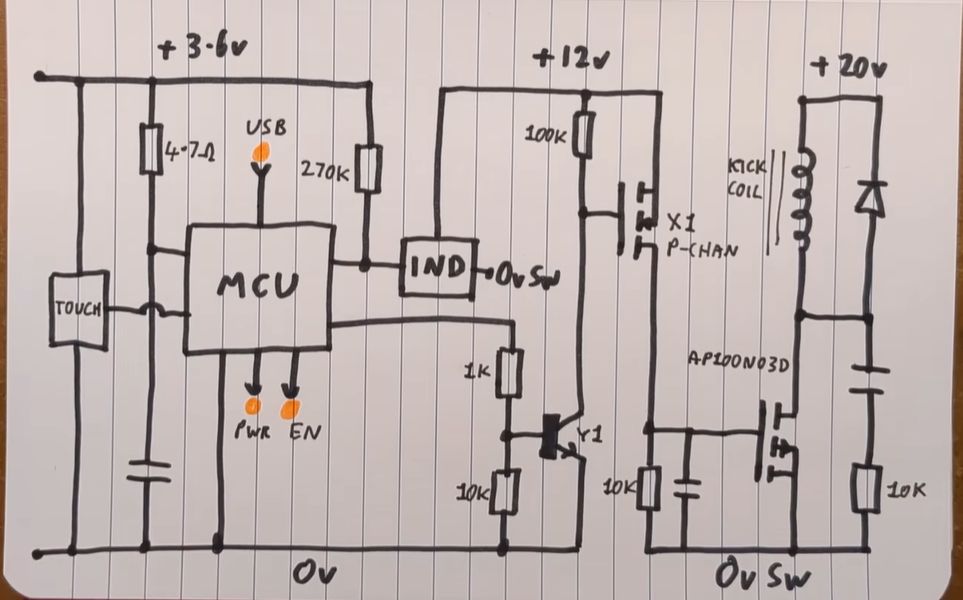
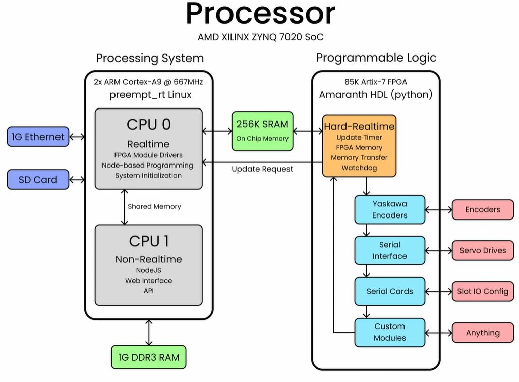
That said, if you’re persistent enough, you can reverse-engineer these beasts to the point where you can develop your own controller hardware and software solution. This is exactly what was done, resulting in an open source controller, found on the ExcessiveMotion GitHub page, that should allow you to control many of these industrial robots. At the core is a Zynq-7000 hybrid FPGA-ARM SoC chip, running real-time Linux (with preemptive scheduling patch) on the SoC side and custom HDL on the FPGA side to handle the hard real-time tasks.
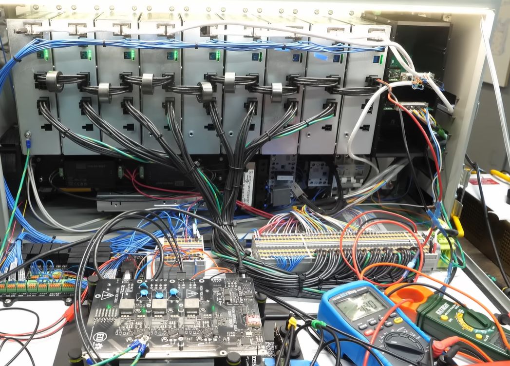
The controller is made to be modular, with a backplane that can accept various interface cards in addition to the current RS-485 and RS-422 interfaces that are commonly used in industrial settings, such as here for controlling the individual servo drives of the robots. To make assembly and testing interesting, the first controller and integration with a robot was made ready for display at the Open Sauce 2025 event, requiring things to be rushed along, including reverse-engineering the servo protocol for a small-ish industrial robot suitable for public display and use, as well as developing the kinematics for the robotic arm.
With the controller now demonstrated, clearly this is the perfect time to rush out and get one of these fun industrial robots for a few hundred bucks. Currently the controller is still being finalized, with the author asking for feedback on what it should be able to support. If you have a particularly unusual industrial robot lounging around without the requisite controller, this might be your chance to revive it.
Thanks to [Hans] for the tip.
Continue reading “Open Source Controller For Old And Expensive Industrial Robots”