Detecting Anti-Neutrinos From Distant Fission Reactors Using Pure Water At SNO+

Although neutrinos are exceedingly common, their near-massless configuration means that their presence is rather ephemeral. Despite billions of them radiating every second towards Earth from sources like our Sun, most of them zip through our bodies and this very planet without ever interacting with either. This property is also what makes studying these particles that are so fundamental to our understanding so complicated. Fortunately recently published results by researchers behind the SNO+ neutrino detector project shows that we may see a significant bump in our neutrino detection sensitivity.

The Sudbury Neutrino Detector (Courtesy of SNO)

In their paper (preprint) in APS Physical Review Letters, the researchers describe how during the initial run of the new SNO+ neutrino detector they were able to detect anti-neutrinos originating from nuclear fission reactors over 240 kilometers away, including Canadian CANDU and US LWR types. This demonstrated the low detection threshold of the  SNO+ detector even in its still incomplete state between 2017 and 2019. Filled with just heavy water and during the second run with the addition of nitrogen to keep out radioactive radon gas from the surrounding rock of the deep mine shaft, SNO+ as a Cherenkov detector accomplished a threshold of 1.4 MeV at its core, more than sufficient to detect the 2.2 MeV gamma radiation from the inverse beta decays (IBD) that the detector is set up for.

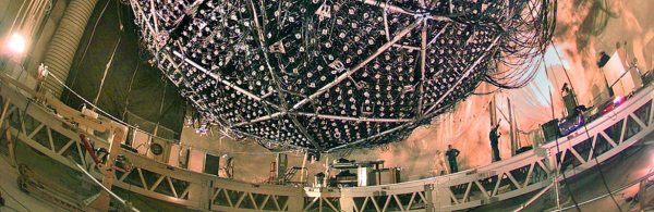
The SNO+ detector is the evolution of the original Sudbury Neutrino Observatory (SNO), located 2.1 km below the surface in the Creighton Mine. SNO ran from 1999 to 2006, and was part of the effort to solve the solar neutrino problem, which ultimately revealed the shifting nature of neutrinos via neutrino oscillation. Once fully filled with 780 tons of linear alkylbenzene as a scintillator, SNO+ will investigate a number of topics, including neutrinoless double beta decay (Majorana fermion), specifically the confounding question regarding whether neutrinos are its own antiparticle or not

The focus of SNO+ on nearby nuclear fission reactors is due to the constant beta decay that occurs in their nuclear fuel, which not only produces a lot of electron anti-neutrinos. This production happens in a very predictable manner due to the careful composition of nuclear fuel. As the researchers noted in their paper, SNO+ is accurate enough to detect when a specific reactor is due for refueling, on account of its change in anti-neutrino emissions. This is a property that does not however affect Canadian CANDU PHWRs, as these are constantly refueled, making their neutrino production highly constant.

Each experiment by SNO+ produces immense amounts of data (hundreds of terabytes per year) that takes a while to process, but if these early results are anything to judge by, then SNO+ may progress neutrino research as much as SNO and kin have previously.

Noninvasive Sensors For Brain–Machine Interfaces Based On Micropatterned Epitaxial Graphene

As fun as brain-computer interfaces (BCI) are, for the best results they tend to come with the major asterisk of requiring the cutting and lifting of a section of the skull in order to implant a Utah array or similar electrode system. A non-invasive alternative consists out of electrodes which are placed on the skin, yet at a reduced resolution. These electrodes are the subject of a recent experiment by [Shaikh Nayeem Faisal] and colleagues in ACS Applied NanoMaterials employing graphene-coated electrodes in an attempt to optimize their performance.

Impedance values of eight-channel FEG and eight-channel HPEG sensor systems placed on the occipital area of the head. (Faisal et al., 2023)

Although external electrodes can be acceptable for basic tasks, such as registering a response to a specific (visual) impulse or for EEG recordings, they can be impractical in general use. Much of this is due to the disadvantages of the ‘wet’ and ‘dry’ varieties, which as the name suggests involve an electrically conductive gel with the former.

This gel ensures solid contact and a resistance of no more than 5 – 30 kΩ at 50 Hz, whereas dry sensors perform rather poorly at >200 kΩ at 50 Hz with worse signal-to-noise characteristics, even before adding in issues such as using the sensor on a hairy scalp, as tends to be the case for most human subjects.

In this study, they created electrode arrays in a number of configurations, each of which used graphene as the interface material. The goal was to get a signal even through human hair — such as on the back of the head near the visual cortex — that would be on-par with wet electrodes. The researchers got very promising results with hex-patterned epitaxial graphene (HEPG) sensors, and even in this early prototype stage, the technique could offer an alternative where wet electrodes are not an option.

While the subject is complex, brain-computer interfaces don’t have to be the sole domain of research laboratories. We recently covered an open hardware Raspberry Pi add-on that can let you experiment with detecting and filtering biosignals from the comfort of your own home.

Uranium-241 Isotope Created And Examined Via Multinucleon Transfer Reactions And Mass Spectrometry

A recent paper (PDF) in Physical Review Letters by T. Niwase and colleagues covers a fascinating new way to both create and effectively examine isotopes by employing a cyclotron and a mass spectrograph. In the paper, they describe the process of multinucleon transfer (MNT) and analysis at the recently commissioned KEK Isotope Separation System (KISS), located at the RIKEN Nishina Center in Japan.

Sketch of the KISS experimental setup. The blue- and yellow-colored areas are filled with Ar and He gases, respectively. Differential pumping systems are located after the doughnut-shaped gas cell as well as before and after the GCCB. (Credit: Niwase et al., 2023)
Sketch of the KISS experimental setup. The blue- and
yellow-colored areas are filled with Ar and He gases, respectively. Differential pumping systems are located after the doughnut-shaped gas cell as well as before and after the GCCB. (Credit: Niwase et al., 2023)

The basic process which involves the RIKEN Ring Cyclotron, which was loaded for this particular experiment with Uranium-238 isotope. Over the course of four days, 238U particles impinged on a 198Pt target, after which the resulting projectile-like fragments (PLF) were led through the separation system (see sketch). This prepared the thus created ions to be injected into the multi-reflection time-of-flight mass spectrograph (MRTOF MS), which is a newly installed and highly refined mass spectrograph which was also recently installed at the facility.

Using this method, the researchers were able to establish that during the MNT process in the cyclotron, the transfer of nucleons from the collisions had resulted in the production of 241U as well as 242U. Although the former had not previously been produced in an experimental setting, the mass of 242U had not been accurately determined. During this experiment, the two uranium as well as neptunium and other isotopes were led through the MRTOF MS instrument, allowing for the accurate measurement of the characteristics of each isotope.

The relevance of producing new artificial isotopes of uranium lies not so much in the production of these, but rather in how producing these atoms allows us to experimentally confirm theoretical predictions and extrapolations from previous data. This may one day lead us to amazing discoveries such as the famously predicted island of stability, with superheavy, stable elements with as of yet unknown properties.

Even if such astounding discoveries are not in the future for theoretical particle physics, merely having another great tool like MNT to ease the burden of experimental verification would seem to be more than worth it.

Building An Electron Microscope For Research

There are a lot of situations where a research group may turn to an electron microscope to get information about whatever system they might be studying. Assessing the structure of a virus or protein, analyzing the morphology of a new nanoparticle, or examining the layout of a semiconductor all might require the use of one of these devices. But if your research involves the electron microscope itself, you might be a little more reluctant to tear down these expensive devices to take a look behind the curtain as the costs to do this for more than a few could quickly get out of hand. That’s why this research group has created their own electron detector.

Specifically, the electron detector is designed for use in a scanning electron microscope, which is typically used for inspecting the surface of a sample and retrieving a high-resolution, 3D image of it compared to transmission microscopes which can probe internal structures. The detector is built on a four-layer PCB which includes the photodiode sensing array, a series of amplifiers, and a power supply. All of the circuit diagrams and schematics are available for inspection as well thanks to the design being licensed under the open Creative Commons license. For any research team looking to build this, a bill of materials is also included, as is a set of build instructions.

While this is only one piece of the puzzle surrounding the setup and operation of an electron microscope, its arguably the most important, and also greatly lowers the barrier of entry for anyone looking to analyze electron microscope design themselves. With an open standard, anyone is free to modify or augment this design as they see fit which is a marked improvement over the closed and expensive proprietary microscopes out there. And, if low-cost microscopes are your thing be sure to check out this fluorescence microscope we featured that uses readily-available parts to dramatically lower the cost compared to commercial offerings.

Self-Cleaning Tech Could Help Solar Panels Keep Efficiency Up

Solar panels are a special kind of magic — turning light into useful electrical energy. However, they don’t work nearly as well when they’re covered in dust, dirt, and grime. Conventional solutions involve spraying panels down with pure water, which is expensive and wasteful, or dry scrubbing, which can cause efficiency loss through scratching the panels. However, innovative new methods may offer useful solutions in this area, as shared by EETimes.

Researchers at MIT have explored the use of electrostatic methods to remove dust from solar panels. By creating a sufficiently strong electrostatic field, dust particles can be compelled to leap off of solar panels. The cleaning method requires no water and is entirely non-contact. It uses a motor system to pass a charged electrode past the surface of the panels, with the opposite charge applied to the panels themselves. This repels the dust from the panels and onto the moving electrode.

Other methods include the use of special “self-cleaning” glass manufactured with a laser etching technique. The method, referred to as Direct Laser Interference Patterning, or DLIP, creates microscopic features on the order of 300 nm to 30 um on the surface of the glass. The pattern creates a so-called “functional surface” from which dirt simply slides off. The laser-etched pattern has no negative impact on transparency.

If these ideas prove practical, expect them to take off quickly. Commercially viable technologies spread fast in the renewable space, as we’ve seen with the rapid uptake of floating solar farms in recent years. 

The Challenges Of Producing Graphene In Quantity

We’ve all heard the incredible claims made about graphene and its many promising applications, but so far the wonder-material has been held back by the difficulty of producing it in large quantities. Although small-scale production was demonstrated many years ago using basic Scotch tape, producing grams or even kilograms of it in a scalable industrial process seemed like a pipedream — until recently. As [Tech Ingredients] demonstrates in a new video, the technique of flash Joule heating of carbon may enable industrial graphene production.

The production of this flash graphene (FG) was first demonstrated by Duy X. Luong and colleagues in a 2020 paper in Nature, which describes a fairly straightforward process. In the [Tech Ingredients] demonstration it becomes obvious how easy graphene manufacturing is using this method, requiring nothing more than carbon black as ingredient, along with a capacitor bank, vacuum chamber and a number of reasonably affordable items.

Perhaps best of all is that no refinement or other complicated processes are required to separate the produced graphene from the left-over carbon black and other non-graphene products. Using multiple of these carbon black-filled tubes in parallel, producing graphene could conceivably be scaled up to industrial levels. This would make producing a few kilograms of graphene significantly easier than coating hard drive platters with the substance.

Continue reading “The Challenges Of Producing Graphene In Quantity”

Busting Wireless ESD Wrist Straps With LTT And ElectroBOOM

Nobody likes getting zapped from an electrostatic discharge, no matter whether you’re a fragile ASIC or a bag-of-mostly-salty-water humanoid. To prevent this, ESD wrist straps and similar are essential tools, as they prevent the build-up of a charge on your humanoid’s skin, essentially like a very large electrolyte-filled capacitor. Yet you can buy wireless ESD straps everywhere that are supposed to somehow dissipate this charge into the ether, even though this would seem to undermine the laws of physics that make capacitors work.

In a practical experimentation and assorted hijinks video collaboration by [Linus] from Linus Tech Tips and [Mehdi Sadaghdar] from ElectroBOOM put these wireless ESD straps to the test, featuring [Mehdi]’s DIY Van de Graaff generator to charge [Linus] up. What is excellently demonstrated in this video is how effective a real ESD strap is, and how the ‘wireless’ version is just a scam that does absolutely nothing to dissipate the charge, being just a waste of a 1 MOhm resistor and what could have been a real ESD strap.

Also covered in the video are what the reason for the resistor in an ESD strap is, and why metal bracelet type ESD straps are not appropriate, for very good reasons.

Continue reading “Busting Wireless ESD Wrist Straps With LTT And ElectroBOOM”