Diamonds are nearly perfect crystals, but not totally perfect. The defects in these crystals give the stones their characteristic colors. But one type of defect, the NV — nitrogen-vacancy — center, can hold a particular spin, and you can change that spin with the correct application of energy. [Asianometry] explains why this is important in the video below.
Interestingly, even at room temperature, an NV center stays stable for a long time. Even more importantly, you can measure the spin nondestructively by detecting light emissions from the center.
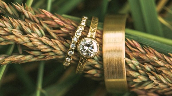
The process of creating a diamond naturally takes between 1 and 3.3 billion years. Conversely, a lab-grown diamond can now be created in 150 minutes. But despite being an ethical and environmentally-friendly alternative to the real thing, the value of lab-grown diamonds has plummeted in recent years. Manufacturers are doing various things to battle the stigma and increase their value by being carbon neutral and using recycled metals.
About halfway through is where this article gets really interesting. Swiss jeweler LOEV has partnered with lab growers Ammil to produce a line of Swiss-made jewelry by relying on renewable energy sources. 90% comes from hydroelectric power, and the rest comes from solar and biomass generation. Now, on to the process itself.
Growing a diamond starts with a seed — a thin wafer of diamond laser-shaved off of an existing stone, and this is placed in a vacuum chamber and subjected to hydrocarbon gas, high heat (900 to 1200 °C), and pressure.
Then, a microwave beam induces carbon to condense and form a plasma cloud, which crystallizes and forms diamonds. The result is called a ‘cake’ — a couple of diamond blocks. The excess carbon is lasered away, then the cake is processed and polished. This is known as the chemical vapor deposition method (CVD).
There is another method of growing diamonds in a lab, and that’s known as the high-pressure, high-temperature (HPHT) method. Here, a small bit of natural diamond is used to seed a chamber filled with carbon, which is then subjected to high pressure and temperatures. The carbon crystallizes around the seed and grows around a millimeter each day.
As the industry evolves, lab-grown diamonds present a sustainable alternative to natural diamonds. But the consumer is always in charge.
The vast majority of semiconductors products we use every day are primarily constructed on a silicon process, using wafers of pure silicon. But whilst the economics are known, and processes mature, there are still some weaknesses. Especially for power applications. gallium nitride (GaN) and silicon carbide (SiC) are materials that have seen an explosion in uses in the power space, driven especially by an increase in electric vehicle sales and other high-power/high-voltage systems such as solar arrays. But, SiC is expensive and very energy intensive. It looks like diamond substrates could become much more common if the work by Diamfab takes off.
Diamond, specifically thin films of synthetic diamond formed on a suitable substrate, exhibits many desirable properties, such as a vastly superior maximum electric field compared with silicon, and a thermal conductivity five times better than copper. Such properties give diamond structures a big power and voltage advantage over SiC, which is in turn a lot better the pure silicon. This also means that diamond-based transistors are more energy efficient, making them smaller and cheaper, as well as better performing. Without the high formation temperatures needed for SiC, diamond could well be their downfall, especially once you factor in the reduced environmental impact. There is even some talk about solid-state, high-voltage diamond insulator capacitors becoming possible. It certainly is an interesting time to be alive!
Aspiring TIG welders very quickly learn the importance of good tungsten electrode grinding skills. All it takes is a moment’s distraction or a tiny tremor in the torch hand to plunge the electrode into the weld pool, causing it to ball up and stop performing its vital function. Add to that the fussy nature of the job — tungstens must only be ground parallel to the long axis, never perpendicular, and at a consistent angle — and electrode maintenance can become a significant barrier to the TIG beginner.
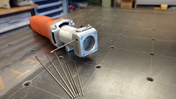
A custom tungsten grinder like this one might be just the thing to flatten that learning curve. It comes to us by way of [The Metalist], who turned an electric die grinder into a pencil sharpener for tungsten electrodes. What we find fascinating about this build is the fabrication methods used, as well as the simplicity of the toolkit needed to accomplish it. The housing of the attachment is built up from scraps of aluminum tubing and sheet stock, welded together and then shaped into a smooth, unibody form that almost looks like a casting. Highlights include the mechanism for adjusting the angle of the grind as well as the clever way to slit the body of the attachment so it can be clamped to the nosepiece of the die grinder. We also thought the inclusion of a filter to capture tungsten dust was a nice touch; most TIG electrodes contain a small amount of lanthanum or thorium, so their slight radioactivity is probably best not inhaled.
We love builds like this that make a tedious but necessary job a little quicker and easier to bear, and anything that stands to make us a better welder — from simple purpose-built fixtures to large-scale rotary tables — is OK in our book.
Even if you’re pretty sure what the answer will be, a marriage proposal is attended by a great deal of stress to make the event as memorable and romantic as possible. You’ve got a lot of details to look after, not least of which is the ring. So why not take some of the pressure off and just 3D-print the thing?
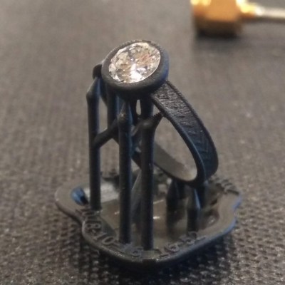
No, a cheesy PLA ring is probably not going to cut it with even the most understanding of fiancees, and that’s not at all what [Justin Lam] did with this DIY engagement ring. He took an engineer’s approach to the problem – gathering specs, making iterative design changes in Fusion 360, and having a prototype ring SLA printed by a friend. That allowed him to tweak the design before sending it off to Shapeways for production. We were surprised to learn that jewelry printing is a big deal, and Shapeways uses a lost-wax process for it. First a high-resolution wax SLA printer is used to make a detailed positive, which is then used to make a plaster mold. The mold is fired to melt the wax, and molten gold is poured in to make the rough casting, which is cleaned and polished before shipping.
Once he had the ring, [Justin] watched a few jewelry-making videos to learn how to set the family heirloom stone into the bezel setting; we admit we cringed a bit when he said he used the blade shaft of a screwdriver to crimp the edge of the bezel to the stone. But it came out great, even if it needed a bit of resizing. The details of the proposal are left to the romantically inclined, but TL;DR – she said yes.
Congratulations to the happy couple, and to [Justin] for pulling off a beautiful build. Most of our jewelry hacks are of the blinkenlight variety rather than fine jewelry, although we have featured a machinist’s take on the subject before.
If you’ve followed any of our coverage of quantum computing, you probably know that the biggest challenge is getting quantum states to last very long, especially when moving them around. Researchers at Princeton may have solved this problem as they demonstrate storing qubits in a lab-created diamond. The actual publication is behind a paywall if you want to learn even more.
Generally, qubits are handled as photons and moved in optical fibers. However, they don’t last long in that state and it is difficult to store photons with correct quantum information. The impurities in diamonds though may have the ability to transfer a photon to an electron and back.
For those not into the anatomy and physiology of semiconductors, getting a look at the inside of the chip can reveal valuable information needed to reverse engineer a device, or it can just scratch the itch of curiosity. Lapping (the gentle grinding away of material) is one way to see the layers that make up the silicon die that lies beneath the epoxy. Hard drives designed to spin at 7200 rpm or more hardly seem a suitable spinning surface for a gentle lapping, but [electronupdate] just wanted the platter for its ultra-smooth, ultra-flat surface.
He removed the heads and replaced the original motor with a gear motor and controller to spin the platter at less than 5 rpm. A small holder for the decapped die was fashioned, and pinched between the platter hub and an idler. It gently rotates the die against the abrasive-covered platter as it slowly revolves. But the die wasn’t abrading evenly. He tried a number of different fixtures for the die, but never got to the degree of precision needed to see through the die layer by layer. We wonder if the weight of the die fixture is deflecting the platter a bit?
Failure is a great way to learn, if you can actually figure out where you went wrong. We look to the Hackaday community for some insight. Check out the video below and sound off in the comments if you’ve got any ideas.