One-key Keyboard Is Exercise In Sub-millimeter Design

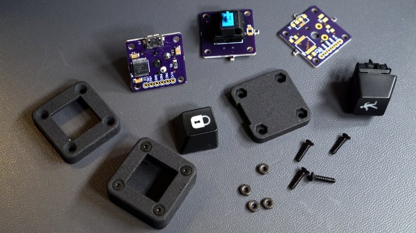
As [Glen] describes it, the only real goal in his decision to design his single-key USB keyboard was to see how small he could build a functional keyboard using a Cherry MX key switch, and every fraction of a millimeter counted. Making a one-key USB keyboard is one thing, but making it from scratch complete with form-fitting enclosure that’s easy to assemble required careful design, and luckily for all of us, [Glen] has documented it wonderfully. (Incidentally, Cherry MX switches come in a variety of qualities and features, the different models being identified by their color. [Glen] is using a Cherry MX Blue, common in keyboards due to its tactile bump and audible click.)

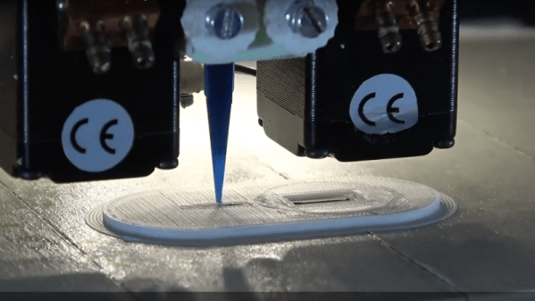
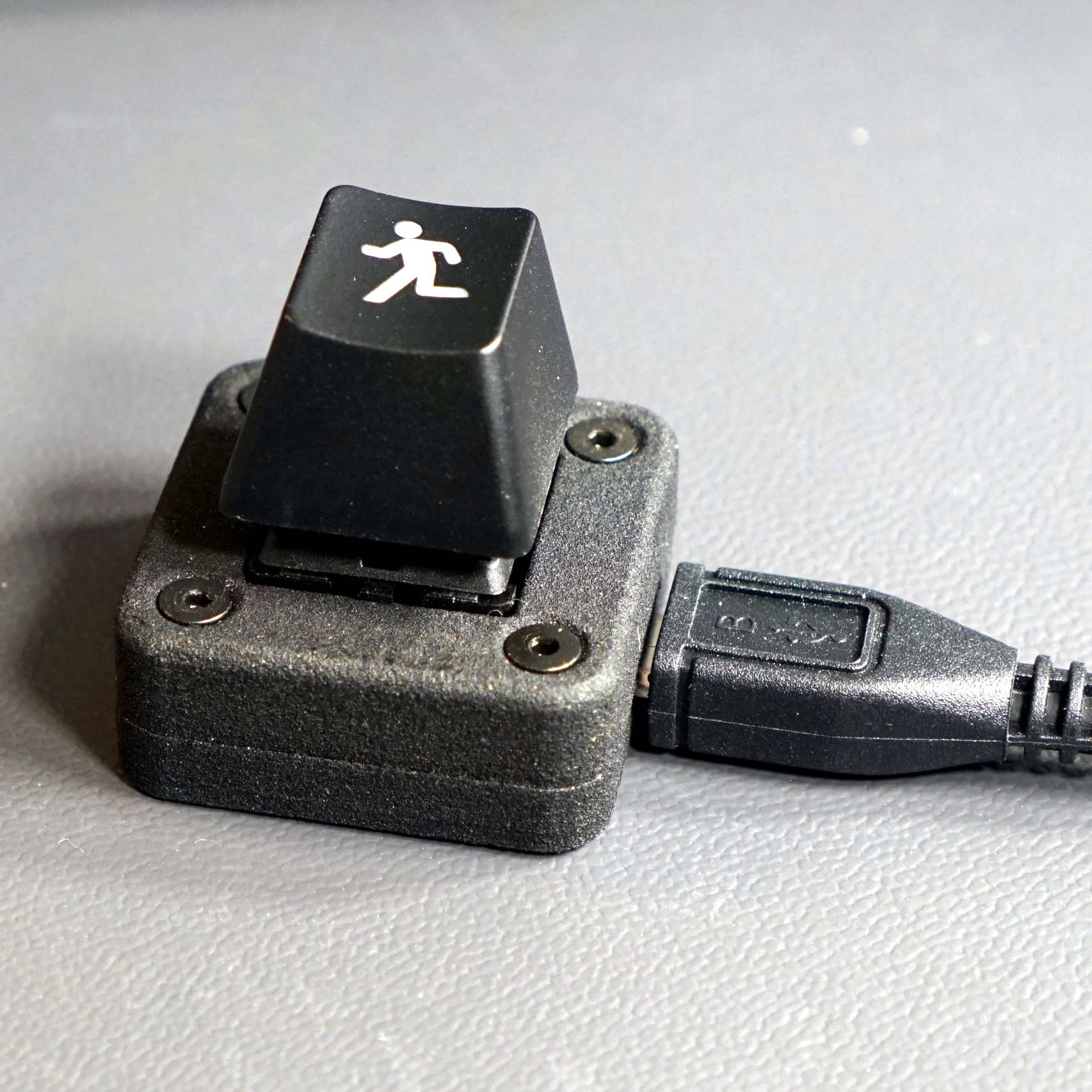
[Glen] steps though the design challenges of making a device where seemingly every detail counts, and explains problems and solutions from beginning to end. A PIC16F1459, a USB micro-B connector, and three capacitors are all that’s needed to implement USB 2.0, but a few other components including LED were added to help things along. The enclosure took some extra care, because not only is it necessary to fit the board and the mounted components, but other design considerations needed to be addressed such as the depth and angle of the countersink for the screws, seating depth and clearance around the USB connector, and taking into account the height of the overmold on the USB cable itself so that the small device actually rests on the enclosure, and not on any part of the cable’s molding. To top it off, it was also necessary to adhere to the some design rules for minimum feature size and wall thicknesses for the enclosure itself, which was SLS 3D printed in nylon.

PCB, enclosure, software, and bill of materials (for single and triple-key versions of the keyboard) are all documented and available in the project’s GitHub repository. [Glen] also highlights the possibility of using a light pipe to redirect the embedded LED to somewhere else on the enclosure; which recalls his earlier work in using 3D printing to make custom LED bar graphs.

PCB Take On Stars, Moons, And Ringed Planets Is Gold

Remember when PCBs were green and square? That’s the easy default, but most will agree that when you’re going to show off your boards instead of hiding them in a case, it’s worth extra effort to make them beautiful. We’re in a renaissance of circuit board design and the amount of effort being poured into great looking boards is incredible. The good news is that this project proves you don’t have to go nuts to achieve great results. This stars, moons, and planets badge looks superb using just two technical tricks: exposed (plated) copper and non-rectangular board outline.

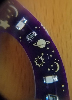
Don’t take that the wrong way, there’s still a lot of creativity that [Steve] over at Big Mess o’ Wires used to make it look this great. The key element here is that copper and solder mask placements have extremely fine pitch. After placing the LEDs and resistors there’s a lot of blank space which was filled with what you might see in the night sky through your telescope.  What caught our eye about this badge is the fidelity of the ringed planet.

The white ink of silk screen is often spotty and jagged at the edges. But this copper with ENIG (gold) plating is crisp through the curves and with razor-sharp tolerance. It’s shown here taken under 10x magnification and still holds up. This is a trick to keep under your belt — if you have ground pours it’s easy to spice up the look of your boards just by adding negative-space art in the solder mask!

[Steve] mentions the board outline is technically not a circle but “a many-sided polygon” due to quirks of Eagle. You could have fooled us! We do like how he carried the circle’s edges through the bulk of the board using silk screen. If you’re looking for tips on board outline and using multiple layers of art in Eagle, [Brian Benchoff] published a fabulous How to do PCB art in Eagle article. Of course, he’s gone deeper than what the board houses offer by grabbing his own pad printing equipment and adding color to white solder mask.

The art was the jumping off point for featuring this badge, but [Steve] is known for his technical dives and this one is no different. He’s done a great job of recounting everything that popped up while designing the circuit, from LED color choice to coin cell internal resistance and PWM to low-power AVR tricks.

Hybrid 3D-Printer Creates Complete Circuits, Case And All

The cool kids these days all seem to think we’re on the verge of an AI apocalypse, at least judging by all the virtual ink expended on various theories. But our putative AI overlords will have a hard time taking over the world without being able to build robotic legions to impose their will. That’s why this advance in 3D printing that can incorporate electronic circuits may be a little terrifying, at least to some.

The basic idea that [Florens Wasserfall] and colleagues at the University of Hamburg have come up with is a 3D-printer with a few special modifications. One is a separate extruder than squirts a conductive silver-polymer ink, the other is a simple vacuum tip on the printer extruder for pick and place operations. The bed of the printer also has a tray for storing SMD parts and cameras for the pick-and-place to locate parts and orient them before placing them into the uncured conductive ink traces.

The key to making the hardware work together though is a toolchain that allows circuits to be integrated into the print. It starts with a schematic in Eagle, which joins with the CAD model of the part to be printed in a modified version of Slic3r, the open-source slicing package. Locations for SMD components are defined, traces are routed, and the hybrid printer builds the whole assembly at once. The video below shows it in action, and we’ve got to say it’s pretty slick.

Sure, it’s all academic for now, with simple blinky light circuits and the like. But team this up with something like these PCB motors, and you’ve got the makings of a robotic nightmare. Or not.

Continue reading “Hybrid 3D-Printer Creates Complete Circuits, Case And All”

Autodesk Introduces Serpentine Router For Eagle

Since Autodesk acquired Eagle a few years ago, they’ve been throwing out all the stops. There is now a button in Eagle that flips your board from the front to the back — a feature that should have been there twenty years ago. There’s parametric part generation, push and shove routing, integration with Fusion 360, and a host of other features that makes Eagle one of the best PCB layout tools available.

Today, Autodesk is introducing something revolutionary. The latest version of Eagle (version 8.7.1) comes with a manual serpentine routing mode, giving anyone the same tools as the geniuses at Nokia twenty years ago.

An exclusive first look at Eagle’s new serpentine routing mode

The new serpentine routing mode is invoked via the SNAKE command. This brings up serpentine routing interface, where you can add nets and place your serpentine router. Click anywhere on the screen, and you can route around pads and traces to collect all the vias, hopefully netting a high score.

There are some tricks to this new mode. Control and Shift change the speed of serpentine routing, and the current zoom level changes the initial speed. As you route between vias, the serpentine router grows longer, making routing significantly more difficult, but if you’re up to the task you’ll eventually get a ‘You’re Winner’ screen.

This is just the innovation we’ve been looking for from Autodesk since their acquisition of Eagle. It’s not push and shove routing, and it’s not parametric part generation. Serpentine routing is the next big thing in EDA tools, and already this routing mode is on the upcoming feature list for KiCad. The KiCad version of serpentine routing will be pronounced, ‘sneak’.

Autodesk Introduces Parametric Part Generation

The hardest part of any PCB design is adding parts and components. You shouldn’t use random part libraries, and creating your own part libraries is just a pain. Why have we endured this pain for so long, especially considering that most components follow a standard? Add in the fact that 3D modeling and rendering a board in a mechanical CAD tool is now a thing, making creating your own part libraries even more involved.

To solve this problem, Autodesk has introduced library.io, a tool to parametrically generate component footprints for Eagle and 3D models for Fusion360. Given that most parts follow a standard — QFP, TO-, DFN, or SOT23 — this is now the easiest way to create a new part in Eagle with its own 3D model that allows you to bring it into mechanical CAD tools.

An overview parametric parts generation is written up on the Autodesk forums, and covers what is possible with this new tool. There are actually two distinct versions, one is a web-based app that allows you to create packages and footprints parametrically in your browser and export them as a library. The other version of the tool is integrated with Eagle and allows you to create a new component parametrically from within Eagle.

This is a far cry from the standard method of creating new footprints. Instead of toiling over a datasheet and dropping correctly sized pads onto a grid, creating a new parametric footprint is as easy as copying a few numbers. In addition to the new parametric design feature, there’s a new tool in Eagle that does away with placing and naming pins for symbols. Now you can simply cut and paste a list of pins from the datasheet.

It should be noted that everything created with the library.io tool can be downloaded and used offline. Combine that with the recent news that KiCad can now ingest Eagle board and schematic files, and you have a way to create parametric footprints in everyone’s favorite Open Source PCB tool as well.

Exporting Eagle Libraries To FOSS Tools

Since Autodesk’s acquisition, Eagle has been making waves in the community. The de facto standard for Open Hardware PCB design is now getting push-and-shove routing, a button that flips the board over to the back (genius!), integration with Fusion360, automated 3D renderings of components, and a bunch of other neat tools. However, Eagle is not without its warts, and there is a desire to port those innumerable Eagle board layouts and libraries to other PCB design packages. This tool does just that.

The tool is an extension of pcb-rnd, a FOSS tool for circuit board editing, and this update massively extends support for Eagle boards and libraries. As an example, [VK5HSE] loaded up an Eagle .brd file of a transceiver, selected a pin header, and exported that component to a KiCad library. It worked the first time. For another experiment, the ever popular TV-B-Gone .brd file was exported directly to pcb-rnd. This is a mostly complete solution for Eagle to KiCad, Eagle to Autotrax, and Eagle to gEDA PCB, with a few minimal caveats relating to copper pours and silkscreen — nothing that can’t be dealt with if you’re not mindlessly using the tool.

While it must be noted that most Open Hardware projects fit inside a 80 cm2 board area, and can therefore be opened and modified with the free-to-use version of Autodesk’s Eagle, this is a very capable tool to turn Eagle boards and libraries into designs that can be built with FOSS tools.

Thanks [Erich] for the tip.

Friday Hack Chat: Eagle One Year Later

Way back in June of 2016, Autodesk acquired Cadsoft, and with it EagleCAD, the popular PCB design software. There were plans for some features that should have been in Eagle two decades ago, and right now Autodesk is rolling out an impressive list of features that include UX improvements, integration with MCAD and Fusion360, and push and shove routing.

Six months into the new age of Eagle, Autodesk announced they would be changing their licensing models to a subscription service. Where you could pay less than $100 once and hold onto version 6.0 forever, now you’re required to pay $15 every month for your copy of Eagle. Yes, there’s still a free, educational version, but this change to a subscription model caused much consternation in the community when announced.

For this week’s Hack Chat, we’re going to be talking about Eagle, one year in. Our guest for this Hack Chat is Matt Berggren, director of Autodesk Circuits, hardware engineer, and technologist that has been working on bringing electronic design to everyone. We’ll be asking Matt all about Eagle, with questions including:

  • What new features are in the latest edition of Eagle?
  • What’s on the Eagle wishlist?
  • What technical challenges arise when designing new features?
  • Where can a beginner find resources for designing PCBs in Eagle?

Join the chat to hear about new features in Eagle, how things are holding up for Eagle under new ownership, and how exactly the new subscription model for Eagle is going. We’re looking for questions from the community, so if you have a question for Matt or the rest of the Eagle team, put it on the Hack Chat event page.

If you’re wondering about how Altium and KiCad are holding up, or have any questions about these PCB design tools, don’t worry: we’re going to have Hack Chats with these engineers in the new year.

join-hack-chat

Our Hack Chats are live community events on the Hackaday.io Hack Chat group messaging. This Hack Chat is going down on noon, PST, Friday, December 15th. Time Zones got you down? Here’s a handy count down timer!

Click that speech bubble to the left, and you’ll be taken directly to the Hack Chat group on Hackaday.io.

You don’t have to wait until Friday; join whenever you want and you can see what the community is talking about.