A metal needle tip comes to a point against a white background. A scale bar in the lower left shows a 300 micrometer length.

Etching Atomically Fine Needle Points

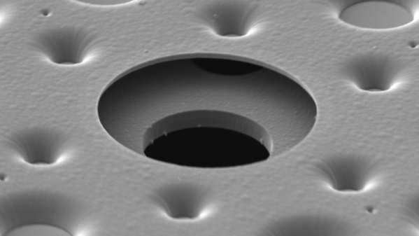
[Vik Olliver] has been extending the lower resolution limits of 3D printers with the RepRapMicron project, which aims to print structures with a feature size of ten micrometers. A molten plastic extruder would be impractical at such small scales, even if a hobbyist could manufacture one small enough, so instead [Vik]’s working on a system that uses a very fine needle point to place tiny droplets of UV resin on a substrate. These points have to be sharper than anything readily available, so his latest experiments have focused on electrochemically etching his own needles.

The needles start with a fine wire, which a 3D-printed bracket holds hanging down into a beaker of electrolyte, where another electrode is located. By applying a few volts across the circuit, with the wire acting as an anode, electrochemical erosion eventually wears through the wire and it drops off, leaving an atomically sharp point. Titanium wire performs best, but Nichrome and stainless steel also work. Copper wire doesn’t work, and by extension, nor does the plated copper wire sometimes sold as “stainless steel” by sketchy online merchants.

The electrolyte was made from either a 5% sodium chloride solution or 1% nitric acid. The salt solution produced a very thin, fine point, but also produced a cloudy suspension of metal hydroxides around the wire, which made it hard to tell when the wire had broken off. The goal of nitric acid was to prevent hydroxide formation; it produced a shorter, blunter tip with a pitted shaft, but it simply etched the tip of the wire to a point, with the rest of the wire never dropping off. Some experimentation revealed that a mixture of the two electrolyte solutions struck a good balance which etched fine points like the pure salt solution, but also avoided cloudy precipitates.

If you’re interested in seeing more of the RepRapMicron, we’ve looked at a previous iteration which scribed a minuscule Jolly Wrencher in marker ink. On a more macro scale, we’ve also seen one 3D printer which used a similar resin deposition scheme.

Simple PCB Agitator Gets The Job Done

These days, PCB fab houses are just about everywhere, and you can’t go buy a taco without walking past eight of them. Still, some out there still like to etch their PCBs at home. If that sounds like you, you might see some value in [Chris Borge]’s PCB agitator. 

The design mostly relies on 3D printed parts, including the main body. It has a heavy base which is filled with concrete to keep it nicely weighed down on the table. A table for holding a PCB and fluid tank is then installed on top, via a bearing which allows it to pivot in one axis. An Arduino Nano commands the agitation of the table top, and hence the PCB etching tank, with a servo used to actually shift the table back and forth.

It’s a simple design — far simpler than some of the advanced coffee-making hardware we’ve seen recently. Regardless, it gets the job done, and done well! In testing, it accelerated [Chris]’s etching jobs significantly, we’re talking hours here. Meanwhile, if you don’t have a 3D printer on hand, you could always try building one out of junk instead!

Continue reading “Simple PCB Agitator Gets The Job Done”

The Best DIY PCB Method?

Now before you start asking yourself “best for what purpose?”, just have a look at the quality of the DIY PCB in the image above. [ForOurGood] is getting higher resolution on the silkscreen than we’ve seen in production boards. Heck, he’s got silkscreen and soldermask at all on a DIY board, so it’s definitely better than what we’re producing at home.

The cost here is mostly time and complexity. This video demonstrating the method is almost three hours long, so you’re absolutely going to want to skip around, and we’ve got some relevant timestamps for you. The main tools required are a cheap 3018-style CNC mill with both a drill and a diode laser head, and a number of UV curing resins, a heat plate, and some etchant.

[ForOurGood] first cleans and covers the entire board with soldermask. A clever recurring theme here is the use of silkscreens and a squeegee to spread the layer uniformly. After that, a laser removes the mask and he etches the board. He then applies another layer of UV soldermask and a UV-curing silkscreen ink. This is baked, selectively exposed with the laser head again, and then he cleans the unexposed bits off.

In the last steps, the laser clears out the copper of the second soldermask layer, and the holes are drilled. An alignment jig makes sure that the drill holes go in exactly the right place when swapping between laser and drill toolheads – it’s been all laser up to now. He does a final swap back to the laser to etch additional informational layers on the back of the board, and creates a solder stencil to boot.

This is hands-down the most complete DIY PCB manufacturing process we’ve seen, and the results speak for themselves. We would cut about half of the corners here ourselves. Heck, if you do single-sided SMT boards, you could probably get away with just the first soldermask, laser clearing, and etching step, which would remove most of the heavy registration requirements and about 2/3 of the time. But if it really needs to look more professional than the professionals, this video demonstrates how you can get there in your own home, on a surprisingly reasonable budget.

This puts even our best toner transfer attempts to shame. We’re ordering UV cure soldermask right now.

Continue reading “The Best DIY PCB Method?”

Up Close And Personal With A MEMS Microphone

If you’ve ever wondered what lies beneath the barely visible hole in the can of a MEMS microphone, you’re in luck, because [Zach Tong] has a $10 pair of earbuds to sacrifice for the cause and an electron microscope.

For the uninitiated, MEMS stands for microelectromechanical systems, the tiny silicon machines that power some of the more miraculous functions of smartphones and other modern electronics. The most familiar MEMS device might be the accelerometer that gives your phone a sense of where it is in space; [Zach] has a deep dive into MEMS accelerometers that we covered a while back.

MEMS microphones seem a little bit easier to understand mechanically, since all they have to do is change vibrations in air into an electrical signal. The microphone that [Zach] tore down for this video is ridiculously small; the SMD device is only about 3 mm long, with the MEMS chip under the can a fraction of a millimeter on a side. After some overall views with the optical microscope, [Zach] opened the can and put the guts under his scanning electron microscope. The SEM shots are pretty amazing, revealing a dimpled silicon diaphragm over a second layer with holes etched right through it. The dimples on the diaphragm nest into the holes, forming an air-dielectric capacitor whose capacitance varies as sound waves vibrate the diaphragm.

The most visually interesting feature, though, might be the deep cavity lying behind the two upper surfaces. The cavity, which [Zach] says bears evidence of having been etched by the deep reactive ion etching method, has cool-looking corrugations in its walls. The enormity of the cavity relative to the thin layers covering it suggests it’s a resonating cavity for the sound waves.

Thanks to [Zach] for this in-depth look at a device that’s amazingly complex yet remarkably simple.

Continue reading “Up Close And Personal With A MEMS Microphone”

Simple Chemistry To Metallize And Etch Silicon Chips

We’ve been eagerly following [ProjectsInFlight]’s stepwise journey toward DIY semiconductors, including all the ups and downs, false leads, and tedious optimizations needed to make it possible for the average hacker to make chips with readily available tools and materials.

Next up is metallization, and spoiler alert: it wasn’t easy. In a real fab, metal layers are added to chips using some form of deposition or sputtering method, each of which needs some expensive vacuum equipment. [ProjectsInFlight] wanted a more approachable way to lay down thin films of metal, so he turned to an old friend: the silver mirror reaction. You may have seen this demonstrated in high school chemistry; a preparation of Tollen’s reagent, a mix of sodium hydroxide, ammonia, and silver nitrate, is mixed with glucose in a glass vessel. The glucose reduces the reagent, leaving the metallic silver to precipitate on the inside of the glass, which creates a beautiful silvered effect.

Despite some issues, the silvering method worked well enough on chips to proceed on, albeit carefully, since the layer is easily scratched off. [ProjectsInFlight]’s next step was to find an etchant for silver, a tall order for a noble metal. He explored piranha solutions, which are acids spiked with peroxide, and eventually settled on plain old white vinegar with a dash of 12% peroxide. Despite that success, the silver layer was having trouble sticking to the chip, much preferring to stay with the photoresist when the protective film was removed.

The solution was to replace the photoresist’s protective film with Teflon thread-sealing tape. That allowed the whole process from plating to etching to work, resulting in conductive traces with pretty fine resolution. Sure they’re a bit delicate, but that’s something to address another day. He’s come a long way from his DIY tube furnace used to put down oxide layers, and suffering through the search for oxide etchants and exploring photolithography methods. It’s been a fun ride so far, and we’re eager to see what’s next.

Continue reading “Simple Chemistry To Metallize And Etch Silicon Chips”

William Blake Was Etching Copper In 1790

You may know William Blake as a poet, or even as #38 in the BBC’s 2002 poll of the 100 Greatest Britons. But did you know that Blake was also an artist and print maker who made illuminated (flourished) books?

Blake sought to marry his art with his poetry and unleash it on the world. To do so, he created an innovative printing process, which is recreated by [Michael Phillips] in the video after the break. Much like etching a PCB, Blake started with a copper sheet, writing and drawing his works backwards with stopping varnish, an acid-resistant varnish that sticks around after a nitric acid bath. The result was a raised design that could then be used for printing.

Cleaning up the ink smudges before printing.

Blake was a master of color, using few pigments plus linseed or nut oil to create pastes of many different hues. Rather than use a brayer, Blake dabbed ink gently around the plate, careful not to splash ink or get any in the etched-away areas. As this was bound to happen anyway, Blake would then spend more time wiping out the etched areas than he did applying the ink.

Another of Blake’s innovations was the printing process itself. Whereas traditionally, illuminated texts must be printed in two different workshops, one for the text and the other for the illustrations, Blake’s method of etching both in the same plate of copper made it possible to print using his giant handmade press.

Want to avoid censorship and print your own ‘zines? Why not build a proofing press?.

Continue reading “William Blake Was Etching Copper In 1790”

Testing Oxide Etchants For The Home Semiconductor Fab

Building circuits on a silicon chip is a bit like a game of Tetris — you have to lay down layer after layer of different materials while lining up holes in the existing layers with blocks of the correct shape on new layers. Of course, Tetris generally doesn’t require you to use insanely high temperatures and spectacularly toxic chemicals to play. Or maybe it does; we haven’t played the game in a while, so they might have nerfed things.

Luckily, [ProjectsInFlight] doesn’t treat his efforts to build semiconductors at home like a game — in fact, the first half of his video on etching oxide layers on silicon chips is devoted to the dangers of hydrofluoric acid. As it turns out, despite the fact that HF can dissolve your skin, sear your lungs, and stop your heart, as long as you use a dilute solution of the stuff and take proper precautions, you should be pretty safe around it. This makes sense, since HF is present in small amounts in all manner of consumer products, many of which are methodically tested in search of a practical way to remove oxides from silicon, which [ProjectsInFlight] has spent so much effort recently to learn how to deposit. But such is the ironic lot of a chip maker.

Three products were tested — rust remover, glass etching cream, and a dental porcelain etching gel — against a 300 nm silicon dioxide layer. Etch speed varied widely, from rust remover’s 10 nm/min to glass etching cream’s blazing 240 nm/min — we wonder if that could be moderated by thinning the cream out with a bit of water. Each solution had pros and cons; the liquid rust remover was cheap easy to handle and clean up, while the dental etching gel was extremely easy to deposit but pretty expensive.

The good news was that everything worked, and each performed differently enough that [ProjectsInFlight] now has a range of tools to choose from. We’re looking forward to seeing what’s next — looks like it’ll be masking techniques.

Continue reading “Testing Oxide Etchants For The Home Semiconductor Fab”