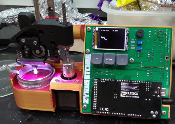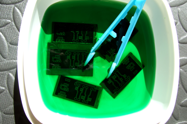
Building circuits on a silicon chip is a bit like a game of Tetris — you have to lay down layer after layer of different materials while lining up holes in the existing layers with blocks of the correct shape on new layers. Of course, Tetris generally doesn’t require you to use insanely high temperatures and spectacularly toxic chemicals to play. Or maybe it does; we haven’t played the game in a while, so they might have nerfed things.
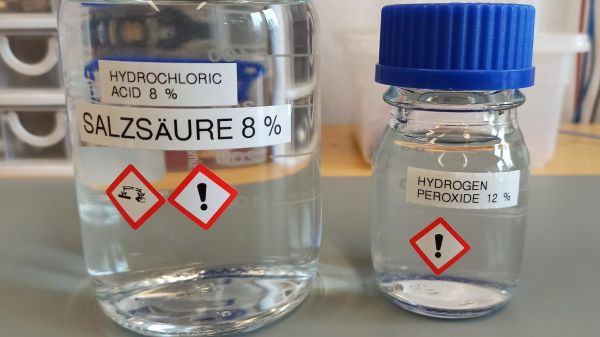
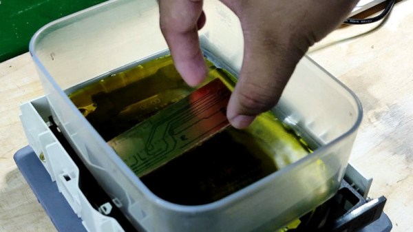
Luckily, [ProjectsInFlight] doesn’t treat his efforts to build semiconductors at home like a game — in fact, the first half of his video on etching oxide layers on silicon chips is devoted to the dangers of hydrofluoric acid. As it turns out, despite the fact that HF can dissolve your skin, sear your lungs, and stop your heart, as long as you use a dilute solution of the stuff and take proper precautions, you should be pretty safe around it. This makes sense, since HF is present in small amounts in all manner of consumer products, many of which are methodically tested in search of a practical way to remove oxides from silicon, which [ProjectsInFlight] has spent so much effort recently to learn how to deposit. But such is the ironic lot of a chip maker.
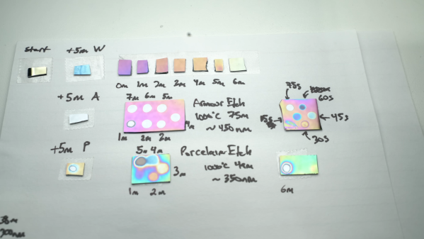
Three products were tested — rust remover, glass etching cream, and a dental porcelain etching gel — against a 300 nm silicon dioxide layer. Etch speed varied widely, from rust remover’s 10 nm/min to glass etching cream’s blazing 240 nm/min — we wonder if that could be moderated by thinning the cream out with a bit of water. Each solution had pros and cons; the liquid rust remover was cheap easy to handle and clean up, while the dental etching gel was extremely easy to deposit but pretty expensive.
The good news was that everything worked, and each performed differently enough that [ProjectsInFlight] now has a range of tools to choose from. We’re looking forward to seeing what’s next — looks like it’ll be masking techniques.
Continue reading “Testing Oxide Etchants For The Home Semiconductor Fab”