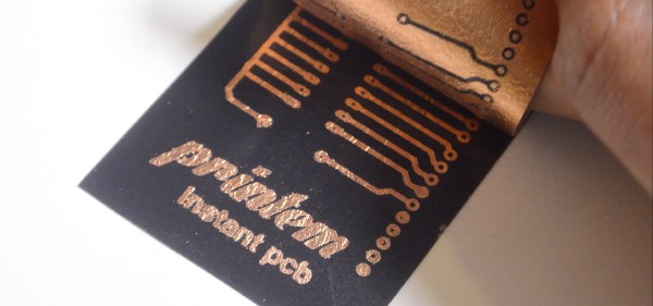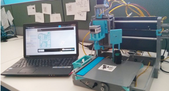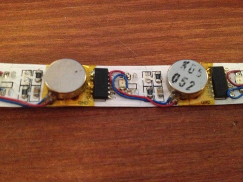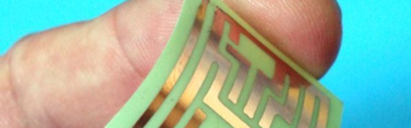
Let’s get it out of the way right up front: you still need to etch the boards. However, [Mikey77] found that flexible plastic (Ninjaflex) will adhere to a bare copper board if the initial layer height is set just right. By printing on a thin piece of copper or conductive fabric, a resist layer forms. After that, it is just simple etching to create a PCB. [Mikey77] used ferric chloride, but other etchants ought to work, as well.
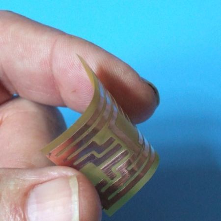
Sound simple, but as usual, the devil is in the details. [Mikey77] found that for some reason white Ninjaflex stuck best. The PCB has to be stuck totally flat to the bed, and he uses spray adhesive to do that. Just printing with flexible filament can be a challenge. You need a totally constrained filament path, for one thing.