Your Battery Holder Is Also Your Power Switch With ToggleSlot

We really like PCB-level hacks, especially ones that show ingenuity in solving a real problem while being super cheap to implement. Hackaday.IO user [Steph] wanted a cheap way to switch a wearable on and off without having to keep popping out the battery, so they came up with a tweaked battery footprint, which is also a simple slide switch.

Most people making badges and wearables will follow the same well-trodden path of just yanking out the cell or placing some cheap switch down and swallowing the additional cost. For [Steph], the solution was obvious. By taking a standard surface-mount CR2032 button cell holder footprint, extending its courtyard vertically, and moving the negative pad up a smidge, the battery can be simply slid up to engage the pad and slid down to disengage and shut off the juice. The spring section of the positive terminal keeps enough pressure on the battery to prevent it from sliding out, but if you are worried, you can always add a dummy pad at the bottom, as well as a little solder bump to add a bit more security.

Now, why didn’t we think of this before? The KiCad footprint file can be downloaded from the project GitHub page, imported into your project and used straight away.

Many of our gadgets are powered by CR2032 cells—so many so that eliminating the need for them leads to interesting projects, like this sweet USB-powered CR2032 eliminator. But how far can you push the humble cell? Well, we held a contest a few years ago to find out!

A graphic showing the suggested footprint dimensions for 0402 parts

Want Better 0402 Reflow? Consider These Footprints!

Assembling with a stencil is just that much more convenient – it’s a huge timesaver, and your components no longer need to be individually touched with a soldering iron for as many times as they have pads. Plus, it usually goes silky smooth, the process is a joy to witness, and the PCB looks fantastic afterwards! However, sometimes components won’t magically snap into place, and each mis-aligned resistor on a freshly assembled board means extra time spent reflowing the component manually, as well as potential for silent failures later on. In an effort to get the overall failure rate down, you will find yourself tweaking seemingly insignificant parameters, and [Worthington Assembly] proposes that you reconsider your 0402 and 0201 footprints.

Over the years, they noticed a difference in failure rates between resistor&capacitor footprints on various boards coming in for assembly – the size and positioning of the footprint pads turned out to be quite significant in reducing failure rate, even on a tenth of millimeter scale. Eagle CAD default footprints in particular were a problem, while a particular kind of footprint never gave them grief – and that’s the one they recommend we use. Seeing the blog post become popular, they decided to share their observations on 0201 as well, and a footprint recommendation too. Are your 0402 resistors giving you grief? Perhaps, checking the footprints you’re using is a good first step.

The 0402 and 0201 components are in a weird spot, where soldering iron assembly is no longer really viable, but the stencil+reflow approach might not be unilaterally successful when you start off – fortunately, that’s where writeups like these come in. Interested in learning stenciling? Get some solder paste, and read up on all the different ways you can put it onto your boards.

Hacked On SO-DIMM Slot Was Worth A Shot

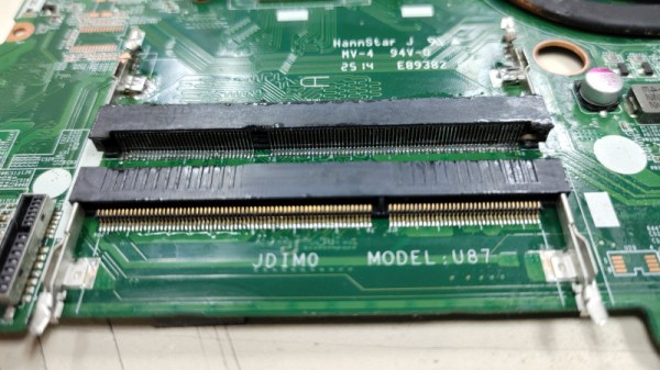
Finding unpopulated pads on a circuit board is often a sign that the device in question has some untapped potential. These blank spots on the board could be left over from features or capabilities that were deleted from the design, or perhaps even represent an optional upgrade that wasn’t installed on this particular specimen. So we certainly understand why [d0rk] was fascinated by the empty SO-DIMM footprint he recently found on a laptop’s motherboard.

The budget Celeron machine shipped with 4 GB of RAM installed in its single socket, a situation [d0rk] hoped he could improve upon with the addition of a second module. But could it really be as simple as pulling the socket from a dead motherboard and soldering it into place? Would other components need to be added to the board? Could the BIOS cope with the unexpected upgrade? There was only one way to find out…

Room to grow

At first, it seemed like the patient didn’t survive the operation. But a close look uncovered that the power button had actually gotten damaged somewhere along the line. Once [d0rk] fixed that the machine started up, but unfortunately the operating system didn’t see the extra RAM module. Even after upgrading the BIOS, the computer remained oblivious to the additional memory.

When he went back in to inspect his solder work for shorts or bad joints, disaster struck. For reasons that aren’t immediately clear, the computer no longer starts. Even after pulling the transplanted SO-DIMM slot off the board entirely, [d0rk] says it won’t make it through the self-test. Obviously a disappointing conclusion, but we respect the effort he put into the attempt.

While this memory upgrade didn’t go according to plan, we’ve seen enough success stories over the years to balance it out. From old wireless routers to cutting-edge video cards, plenty of gadgets have received a memory boost courtesy of a soldering iron and a steady hand.

[Thanks to Timothy for the tip.]

Autodesk Introduces Parametric Part Generation

The hardest part of any PCB design is adding parts and components. You shouldn’t use random part libraries, and creating your own part libraries is just a pain. Why have we endured this pain for so long, especially considering that most components follow a standard? Add in the fact that 3D modeling and rendering a board in a mechanical CAD tool is now a thing, making creating your own part libraries even more involved.

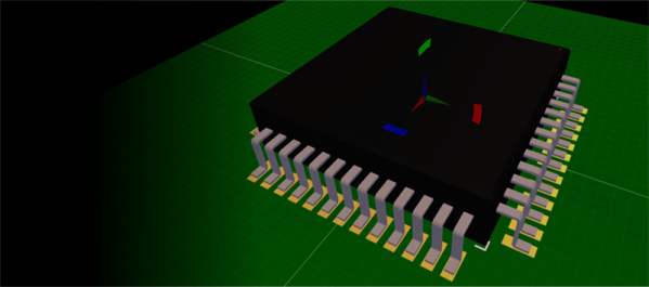
To solve this problem, Autodesk has introduced library.io, a tool to parametrically generate component footprints for Eagle and 3D models for Fusion360. Given that most parts follow a standard — QFP, TO-, DFN, or SOT23 — this is now the easiest way to create a new part in Eagle with its own 3D model that allows you to bring it into mechanical CAD tools.

An overview parametric parts generation is written up on the Autodesk forums, and covers what is possible with this new tool. There are actually two distinct versions, one is a web-based app that allows you to create packages and footprints parametrically in your browser and export them as a library. The other version of the tool is integrated with Eagle and allows you to create a new component parametrically from within Eagle.

This is a far cry from the standard method of creating new footprints. Instead of toiling over a datasheet and dropping correctly sized pads onto a grid, creating a new parametric footprint is as easy as copying a few numbers. In addition to the new parametric design feature, there’s a new tool in Eagle that does away with placing and naming pins for symbols. Now you can simply cut and paste a list of pins from the datasheet.

It should be noted that everything created with the library.io tool can be downloaded and used offline. Combine that with the recent news that KiCad can now ingest Eagle board and schematic files, and you have a way to create parametric footprints in everyone’s favorite Open Source PCB tool as well.

Scanning Parts Into KiCad

You do not know how to make a PCB unless you can make your own parts. [Jan] knows this, but like everyone else he checked out the usual online sources for a footprint for an SD card socket before making his own. It turns out, this SD card socket bought from an online marketplace was completely undocumented. Not only was an Eagle or KiCad footprint unavailable, but CAD files showing the dimensions of the part were non-existent. A solution had to be devised.

Instead of taking calipers and finely measuring all the pads on this SD card socket – a process that would surely fail – [Jan] decided to use a flatbed scanner to trace out the part. The part was placed on the glass and scanned at 300 dpi with a convenient reference object (a public transport card) in the same picture. This picture was imported into a CAD package, scaled to the correct ratio, and exported as a DXF. Since KiCad readily accepts importing DXFs, the CAD file was easily accessed, traced over, and a new part created.

From start to finish, making the footprint for this no-name, off-brand SD card socket took fifteen minutes. That’s nothing compared to the time it would take to manually measure each of the pads, draw a footprint, and print out the footprint at 1:1 scale to see if it matched up several times. It’s awesome work, and a great reminder that the best tools are usually right in front of you.

Assigning New Packages To Eagle PCB Components

adafruit-eagle-component-creation-tut

If you’ve spent any time at all laying out your own circuit boards we’re sure you’ve run into the issue of not having the right component or package available in the standard libraries. If it’s a common part, chances are the symbol definition will be there.  But perhaps the footprint you want to use is missing? Here’s an easy to follow tutorial which demonstrates how to assign new packages to existing Eagle PCB components. It even shows the basics of how to tweak the footprint to fit your needs (like making SMD footprints easier to hand solder).

This will not teach you how to make your own custom symbols, or how to build packages from scratch. But it will let you locate the package you want to use from a different component, then copy it to your own library for use with different parts. And the techniques shown make this a quick and relatively painless process.

We certainly don’t want to start another comment quagmire like the recent PIC v. AVR discussion. But we’ve used both Kicad and Eagle rather extensively and feel that neither one has really mastered part/footprint creation in a user-friendly way. We like Kicad’s total separation of footprints from components, and it’s myriad of parameters which can be used to tweak the layout. But if you use the same components frequently, Eagle’s standard of linking parts and footprints does end up saving a lot of time. What do you think?

Reverse Engineering Salvaged Part Footprints

reverse-engineering-component-footprints

So you just pulled a fancy component off of a board from some broken electronics and you want to use it in your own project. What if the data sheet you found for it doesn’t include measurements for the footprint? Sure, you could pull out your digital calipers, but look at the measurements in the image above. How the heck are you supposed to accurately measure that? [Steve] found an easy answer for this problem. He uses microscope software to process an image of the board.

One common task when working with a microscope is measuring the items which are being viewed under magnification. [Steve] harnessed the power of a piece of free software called MiCam. One of its features is the ability to select an area of the photograph so serve as the measuring stick. To get the labels seen in the image above he selected the left and right edges of the board as the legend. He used his digital calipers to get a precise measurement of this area, then let the software automatically calculate the rest of the distances which he selected with his cursor.

MiCam is written for Windows machines. If you know of Linux or OSX alternatives please let us know in the comments.