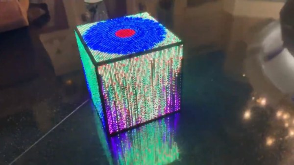
Hidden LED Video Wall At The Oregon Museum Of Science

Glowing and blinking things are some of our favourite projects around these parts, and the bigger, the better. [Thomas] wrote to us recently to share the design and construction of a large LED wall at the Oregon Museum of Science, and the results are nothing short of impressive.

The concept involved a large LED wall that would be completely hidden when switched off. The team decided to approach this by hiding high-brightness LED panels using APA102 strings behind milky-white plexiglass panels covered with a woodgrain print. The screen has a total of 90,000 pixels, arranged in a 408×220 resolution display.

A lot of bespoke LED displays have some pre-coded patterns, or perhaps some basic reactive features. In this case, FPGA grunt was brought to bear on the problem and the display accepts standard HDMI input. Four Spartan 6 Mojo FPGA boards split up the task of addressing the panels, each receiving the same HDMI signal, but only crunching the pixels relevant to their area of the display. To make sure clean SPI signals get to each panel, special RS485 driver chips are used to send the signal over a differential pair from the FPGA, before breaking the signal back out to standard SPI at the destination.

Building such a large display takes special techniques, and [Thomas] notes that the help of a local construction company was imperative to making the construction of the final video wall look easy. It’s always interesting to see what goes into these large installations. Sometimes, a major build can even clear out world stocks of important components.

Hackaday Podcast 002: Curious Gadgets And The FPGA Brain Trust

In this week’s podcast, editors Elliot Williams and Mike Szczys look back on favorite hacks and articles from the week. Highlights include a deep dive in barn-door telescope trackers, listening in on mains power, the backstory of a supercomputer inventor, and crazy test practices with new jet engine designs. We discuss some of our favorite circuit sculptures, and look at a new textile-based computer and an old server-based one.

This week, a round table of who’s-who in the Open Source FPGA movement discusses what’s next in 2019. David Shah, Clifford Wolf, Piotr Esden-Tempski, and Tim Ansell spoke with Elliot at 35C3.

Take a look at the links below if you want to follow along, and as always, tell us what you think about this episode in the comments!

Direct download (60 MB or so.)

Continue reading “Hackaday Podcast 002: Curious Gadgets And The FPGA Brain Trust”

ULX3S: An Open-Source Lattice ECP5 FPGA PCB

The hackers over at Radiona.org, a Zagreb Makerspace, have been hard at work designing the ULX3S, an open-source development board for LATTICE ECP5 FPGAs. This board might help make 2019 the Year of the Hacker FPGA, whose occurrence has been predicted once again after not quite materializing in 2018. Even a quick look at the board and the open-source development surrounding it hints that this time might be different.

Bottom side of ULX3S PCB

The ULX3S was developed primarily as an educational tool for undergraduate-level digital logic classes. As such, it falls into the “kitchen sink” category of FPGA boards, which include a comprehensive suite of peripherals and devices for development, as opposed to more bare-bones FPGA breakouts. The board includes 32 MB SDRAM, WiFi via an ESP-32 (supporting over-the-air update), a connector for an SPI OLED display, USB, HDMI, a microSD slot, eight channels of 12-bit ADC (1 MS/s), a real-time-clock, 56 GPIO pins, six buttons, 11 LEDs, and an onboard antenna for 433 MHz FM/ASK. This seems like a great set of I/Os for both students and anyone else starting FPGA development.

The ULX3S supports members of the Lattice ECP5 FPGA family, ranging from the 12F (12 k LUTs) to the 85F (84 k LUTs). What can you do with this much FPGA horsepower? Have a look at the long list of examples curated in the ULX3S Links repo. There, you’ll find code from retro-computing to retro-gaming, the usual LED and HDMI demos, and even Linux running on a mor1kx OpenRISC core. Maybe the most interesting links in the repo, however, are those that show how to program the FPGA with a completely open-source toolchain. Proprietary toolchains are the last link keeping some vendor’s FPGAs from wider adoption in the OSHW community, and it’s great to see people chipping away at them.

The board itself is completely open-source. In the GitHub repo, you’ll find the KiCAD 5 design files for the PCB released under an MIT-style license. Even more impressive is the advice in the README, which not only welcomes independent production of the boards, but gives some solid advice on dealing with PCBA vendors during manufacture. Our own advice is to do the right thing and offer the developers a cut if you decide to independently market this board, even though you aren’t required to by the license. If want one, but don’t want to manufacture your own, you can contact the developers using the email or gitter links at the bottom of the ULX3S page: they’re currently doing a small production run.

The Radiona Org folks have created a few videos showcasing example code. Check out how the on-board ESP-32 runs a web server that can load bitstreams into the FPGA (in this case for some retro-gaming), after the break.

Continue reading “ULX3S: An Open-Source Lattice ECP5 FPGA PCB”

Pac-Man Fever Comes To The Pano Logic FPGA

If you’ve been reading Hackaday for a while now, you might recall the tale of Pano Logic that we first covered all the way back in 2013. They were a company that put out some very interesting FPGA-based thin clients, but as occasionally happens in situations like this, the market wasn’t ready and the company went belly up. These thin clients, now without official support, invariably got dumped onto the second-hand market. Shame for Pano Logic and their staff, but good news for hackers like [Skip Hansen].

After seeing a few posts about the Pano Logic devices and general FPGA hacking, he decided to grab a few on eBay and dive in. Using open source tools and the wealth of information that’s available [Skip] was able to get a Pac-Man simulator up and running over his holiday break, and he tells us his life may never be the same again. FPGA hacking is a fascinating subject with a lot of activity right now, and since you can get these Pano Logic boxes on eBay for less than $10 USD in some cases, now is as good a time as ever to get your feet wet.

Like many open source projects, [Skip] says his code is built upon the existing work of a number of other programmers, which let him get up and running much faster than if he had to start from scratch. He describes his code as the “glue” that mashes these projects together, but we think he’s being somewhat modest there. It took more than copying and pasting some code into an IDE to get Blinky, Pinky, Inky and Clyde doing their thing on the Pano Logic.

The biggest challenge was the lack of I/O. The Pano Logic thin clients have USB ports, but it seems nobody has quite figured out how to get them working yet. To talk to the outside world, you’ve got to get a little more creative. Eventually [Skip] was able to track down four lines he could effectively use as GPIO: two which are used to drive the LEDs on the device, and two which are used for the VGA port’s Display Data Channel (DDC) pins. Soldering jumpers from the LEDs to the unused pins in the device’s VGA connector meant he was even able to get these four GPIO lines accessible from the outside of the Pano Logic without having to cut any holes in the case.

Anyone with a Pano Logic client that has a VGA port, an Atari 2600 joystick, and who doesn’t mind soldering a couple of wires can now play Pac-Man with the bitstream [Skip] has provided. But where do we go from here? How long until we see DOOM running on it? Perhaps one of you fine readers should pick one up and see what you can do to advance the state of Pano Logic hacking. Just be sure to let us know about it.

We’ve previously covered one of the projects used to get this Pac-Man simulator off the ground, a very cool ray tracing demo for the Pano Logic developed by [Tom Verbeure]. In fact, [Skip] says that project was what got him interested in FPGA hacking in the first place. If you’re thinking of following his lead, you might also want to check out our FPGA Boot Camp.

Wooden Clock To FPGA Conversion

[John] wanted a project to help him learn more about FPGAs. So he started with his wooden clock — made with an Arduino — and ported it over to a Lattice FPGA using Icestorm. What’s nice is that he takes you through the steps he used to simulate the design using the Falsted simulator and then realizing it in the FPGA. Since he’s just starting out, it is a good bet he ran into the same rough edges you will (or did) and sometimes that can really help get you over the hump. You can see a video below, and the code for the project is on GitHub.

For example, after mocking up a circuit design in Falstad he realized he could make one large counter instead of several modules, and he contrasts that to a more modular approach. He also ran into a feature that was simple for the Arduino but difficult for the FPGA. He got it working, but it took some optimization effort to make everything fit in the relatively small FPGA he was using.

Continue reading “Wooden Clock To FPGA Conversion”

How A Microcontroller Hiding In A USB Port Became An FPGA Hiding In The Same

When you think of microcontroller development, you probably picture either a breadboard with a chip or a USB-connected circuit board. But Tim Ansell pictured an ARM dev board that is almost completely hidden inside of a USB port. His talk at the 2018 Hackaday Superconference tells that story and then some. Check out the newly published video, along with more details of the talk, after the break.

Continue reading “How A Microcontroller Hiding In A USB Port Became An FPGA Hiding In The Same”

Old Game Development IDE Goes FPGA

If you have a thing for old game development — things like the Atari 2600 or similar period arcade games — you might already know about the 8bitworkshop IDE. There you can develop code in your browser for those platforms. In a recent blog post, the site announced you can now also do FPGA development in the IDE.

According to the site:

Most computers are fast enough to render a game at 60 Hz, which requires simulating Verilog at almost 5 million ticks per second.

To activate Verilog, you need to select the hamburger menu to the top left, select Platform, and then under Hardware, check Verilog. What makes this different from, say, EDA Playground, is that the output can be waveforms or the output to a virtual TV monitor. For example, here’s one of the examples:

The Verilog code is generating horizontal and vertical sync along with an RGB output and the results appear on the monitor to the right. There is a handle at the bottom of the screen. If you drag it up you will see the logic analyzer output. Drag it down and you’ll see the screen again. The examples include an 8-bit and 16-bit CPU, and example games that can even read the mouse.

Honestly, we don’t think anyone would suggest using Verilog to write in-browser games. That isn’t really the point here. However, if you are trying to learn Verilog, it is great fun to be able to produce something other than just abstract waveforms from simulation. The only downside is that to move to a real piece of hardware, you’d need to duplicate the interfaces provided by the IDE. That would not be very hard, and — of course — if you are just using it to learn you can try a different project for the real world.

If you need help getting going in Verilog, we have a series of boot camps that can help. Those tutorials use EDA Playground, but they’d probably work here, too. If you try them in the IDE, be sure to let us know your experience.