Oscilloscope Clocks: Now In Color!

Ordinarily, when we hear the words “clock” and “oscilloscope” in the same sentence we conjure images of measuring a stable, repeating square wave that acts as the heartbeat of a system. Of course, that’s not the only meaning– there’s a much more fun and less useful one: using an oscilloscope to display the time.

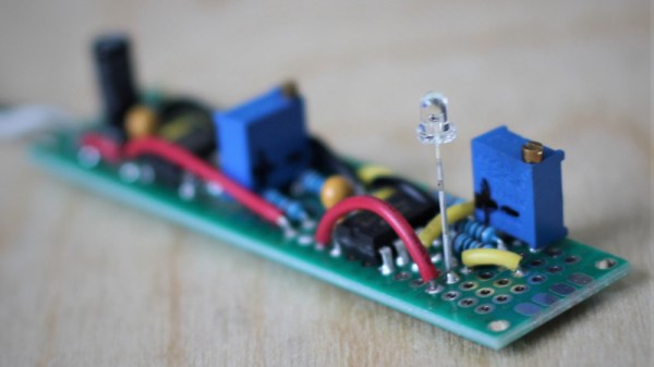
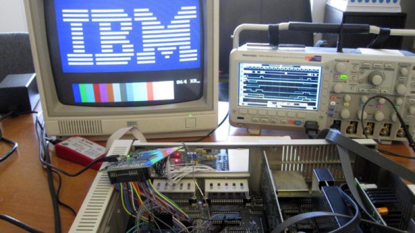
That’s what [Wolfgang Friedrich] set out to do when he cobbled some protoboard, probes, and an FPGA into the Multi Color Oscilloscope Clock. Each digit on the clock is treated like a seven-segment display, made up of three horizontal bars and four vertical bars. The horizontal bars are generated by constant voltage at different levels, and the vertical bars are generated by quickly switching between two voltages. [Wolfgang] decided to use an R-2R resistor ladder DAC to create the appropriate analog signals from the FPGA’s digital outputs. For bonus points, each set of digits (hours, minutes, and seconds) are output concurrently through separate channels, so they can be displayed in different colors on the screen of his four-channel scope (the fourth channel is used for the points between numbers).

Misusing oscilloscopes in the name of fun has become a time-honored tradition– from Tennis for Two back in 1958 (which later became the beloved Pong) to the plethora of analog o-scope clocks we’ve seen, it’s clear that hackers just can’t get enough of the unique vector display style that a scope can provide. We love [Wolfgang]’s idea of using the scope’s channels to create a multi-color display, and we’re left wondering what kind of wacky waveforms we’ll be seeing next.

Capacitive Touch Controller For FPGAs

Most projects that interface with the real world need some sort of input device. Obviously this article is being written from a standardized “human interface device” but when the computers become smaller the problem can get more complicated. We can’t hook up a USB keyboard to every microcontroller since we often only need a few buttons, but even buttons can be a little bit too cumbersome for some applications. For something even simpler, we would like to turn your attention to capacitive touch controllers.

Granted, these devices are really only simpler from a hardware perspective. Rather than a switch that can be prone to failure either when its moving parts break or its contacts become corroded, a capacitive touch button only needs a certain conductive area on something like a PCB, along with a few passive components, to work. The real difficulty is in the software, so this project aims to make it simpler to bring these sort of devices to any FPGA that needs some sort of interface like this. It can operate in stand-alone mode or in a custom user interface, and was written to be platform-independent in VHDL without the need for any dependencies or macros.

The project’s page goes into a great amount of detail on how capacitive touch sensors like these work in general, and describes the operation of this specific code as well. Everything is open source, so it’s ready to be put to work right away. If you need capacitive touch capabilities on something like a microcontroller, though, take a look at this tiny Atmel-powered musical instrument instead.

PS/2 wireless dongle

The Wireless PS/2 Keyboard That Never Was

The PS/2-style port was once about as ubiquitous on PCs as USB connectors are today, and more than a few of us accumulated a fair collection of keyboards and mice that sported the 6-pin mini-DIN plug. They’re not nearly as common today, but when you need one, you need one, so if your stockpile of PS/2 keyboards has dwindled to nothing, you might want to look at rolling your own PS/2 remote keyboard dongle.

That backstory on [Remy Sharp]’s build starts with his acquisition of a neptUNO, a 160€ FPGA retrocomputer that gives you access to just about every Z80 and 6502 computer of yesteryear. While the box supports USB keyboards, [Remy] had trouble getting one to work. So out came a Wemos D1 Mini, which was wired up to a stub of PS/2 cable. The microcontroller is powered by the PS/2 port, and connects to the WiFi network on boot-up and starts a WebSocket server. It also served up a page of HTML, which lets him connect with any device and send keystrokes to the neptUNO. He also added a couple of hardware buttons to the dongle, to access menus on the neptUNO directly. The video below shows it in action.

Perhaps unsurprisingly, [Remy] says he took inspiration for this build from [Ben Eater]’s excellent PS/2 deep dive. We’d like to think he saw that here first, but either way, it’s a valuable reference on how keyboards used to work.

Continue reading “The Wireless PS/2 Keyboard That Never Was”

Here’s A 100 MHz Pin-Compatible 6502 Replacement

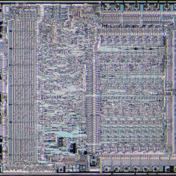
The MOS Technology 6502 CPU was a popular part in its day. In various modified versions, it powered everything from the Commodore 64 to the Nintendo Entertainment System, and showed up in a million other applications too. A popular variant is the 65C02, and [Jürgen] decided to whip up a pin-compatible FPGA version that runs at a blazing 100MHz.

The CPU core was borrowed from work by [Arlet Ottens] and extended with 65C02 functionality by [Ed Spittles] and [David Banks]. [Jürgen] then packaged that core in a Spartan-6 FPGA and placed it on a small PCB the size of the original 65C02’s 40-pin dual inline package.

The FPGA is set up to access the external CPU bus with the timing matched to the clock of the host machine. However, internally, the CPU core runs at 100MHz. It copies RAM and ROM from the host machine into its own internal 64 kilobyte RAM, minus the areas used for memory-mapped I/O by the host. The CPU then runs at full 100MHz speed except when it needs to talk to those I/O addresses.

It allows the chip to accelerate plenty of tasks without completely flipping out when used with older hardware that can’t run at anywhere near 100MHz. The pin-compatible design has been tested successfully in an Apple II and a Commodore 8032, as well as a variety of vintage chess computers.

We’ve seen the opposite before too, with a real 6502 paired with a FPGA acting as the rest of the computer. If you’ve got any cutting-edge 6502 hacks of your own (not a misprint!), let us know!

[Thanks to David Palmer for the tip]

A Game Boy connected to a monitor while playing Super Mario Land 2

FPGA Boards Add VGA And HDMI Interfaces To The Original Game Boy

The classic Game Boy remains a firm favorite in the realm of retrocomputing. Revolutionary as it was at the time, by today’s standards its display is rather primitive, with no backlight and a usable area measuring only 47 mm x 44 mm. [Martoni] figured out a way to solve this, by developing GbVGA and GbHdmi, two projects that enable the Game Boy to connect to an external monitor. This way, you can play Super Mario Land without straining your eyes, and we can also image potential uses for those who stream their gameplay online.

A Game Boy connected to a monitor while playing Super Mario Land 2 Getting the image data out of the Game Boy is surprisingly straightforward, and has been done a few times before. Basically, the connection between the CPU and the LCD screen is a serial interface with a 4 MHz clock, two data lines and two sync lines. [Martoni] uses pin headers sticking out of the Game Boy’s plastic case to connect these to a small FPGA board. The board in question is a Fireant for the VGA version and a Tang Nano 4K for the HMDI model. In either case the FPGA reads out each frame from the Game Boy’s LCD interface and draws the extracted image onto the monitor, using the same four shades of green as used on the original screen.

[Martoni] states that the ultimate goal of these projects is to make a Switch-like docking station for the original Game Boy, which is definitely something we’re looking forward to. Although adding external monitors to the Game Boy is not entirely new, we like the simplicity of this implementation and the fact that anyone can improve upon it thanks to the full source code being available. Similar hacks have been performed on the newer Game Boy Pocket and Game Boy Advance as well.

RISC-V In… Typescript?

We are accustomed to seeing RISC-V implementations in Verilog or VHDL, but [Low Level JavaScript] has one in TypeScript. Before you dismiss it as a mere emulator, know that the project relies on gateware-ts, a conversion between TypeScript and Verilog. From there, you can actually put the CPU on an FPGA. You can see the launch video below and there is one development video as well as, presumably, more to come.

We aren’t sure if many FPGA designers will be willing to switch to TypeScript. But if you are comfortable with it, it might open up FPGA development without having to learn as much of a new language.

Continue reading “RISC-V In… Typescript?”

FPGA Retrocomputer: Return To Moncky

Part of the reason that retrocomputers are still so popular despite their obsolescence is that it’s possible to understand the entire inner workings of a computer like this, from the transistors all the way up to the software. Comparatively, it will likely be a long time (if ever) before anyone is building a modern computer from discrete components. To illustrate this point, plenty of 8-bit computers are available to either restore from original 80s hardware or to build from kits. And if you’d like to get even deeper into the weeds you can design your own computer including the instruction set completely from the ground up using an FPGA.

This project, called the Moncky project, is a step above the usual 8-bit computer builds as it is actually a 16-bit computer. It is built around an Arty Spartan-7 FPGA dev board running around 20 MHz and has access to 2 x 128 kB dual-port RAM for memory. To access the outside world there is a VGA output, PS/2 capability, SPI, and uses an SD card as a hard drive. This project really shines in the software, though, as the project creator [Kris Demuynck] builds everything from scratch in order to illustrate how everything works for educational purposes, and is currently working on implementing a C compiler to make programming the computer easier.

All of the project files, as well as all of the code, are available on the project’s GitHub page if you’d like to follow along or build on this homebrew 16-bit computer. It’s actually the third iteration of this computer, with the Moncky-1 and Moncky-2 being used to develop the more basic building blocks for this computer. While it’s not the first 16-bit computer we’ve seen implemented on an FPGA, it is one of the few that builds its own RISC instruction set and associated software rather than cloning a known existing processor. We’ve also seen some interesting x86 implementations on an FPGA as well.

Thanks to [koen-ieee] for the tip!