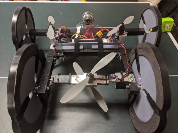
Gravity is a nice thing to have most of the time, but sometimes it would be nice to be able to ignore it for certain applications. Rock climbing, for example, would be much easier, as would performing bridge inspections in the way that a group of mechanical engineering cadets (students) at The Citadel, a military college in South Carolina, were tasked with doing. Frustrated with the amount of traffic backups that normal bridge inspections caused, they invented a robot that defies gravity, and won a $10k prize for their efforts.
The result is essentially an RC car with a drone built in, or looking at it another way it’s a drone with wheels. The car is able to drive on vertical surfaces to inspect the bridges by using its propellers to force itself onto the surface. The lack of complicated moving parts or machinery, like a cable suspension system or other contraption, makes this device exceptionally versatile for the task at hand, reduces the amount of time needed for inspections, and can do them more safely and without closing lanes of traffic. The group hopes to build a second prototype soon and present it to the Department of Transportation for approval for more widespread use.
The need for tools like these is in high demand now as well, especially in the United States where crumbling infrastructure is often not thought about, taken seriously, or prioritized. Even for bridges that aren’t major pieces of infrastructure, tools like these will prove to be very useful.
Thanks to [Ben] for the tip!

